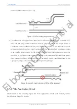
PCB, such as reference layer thickness, number of layers and stacking. Different
reference GND layer will lead to different routing design.
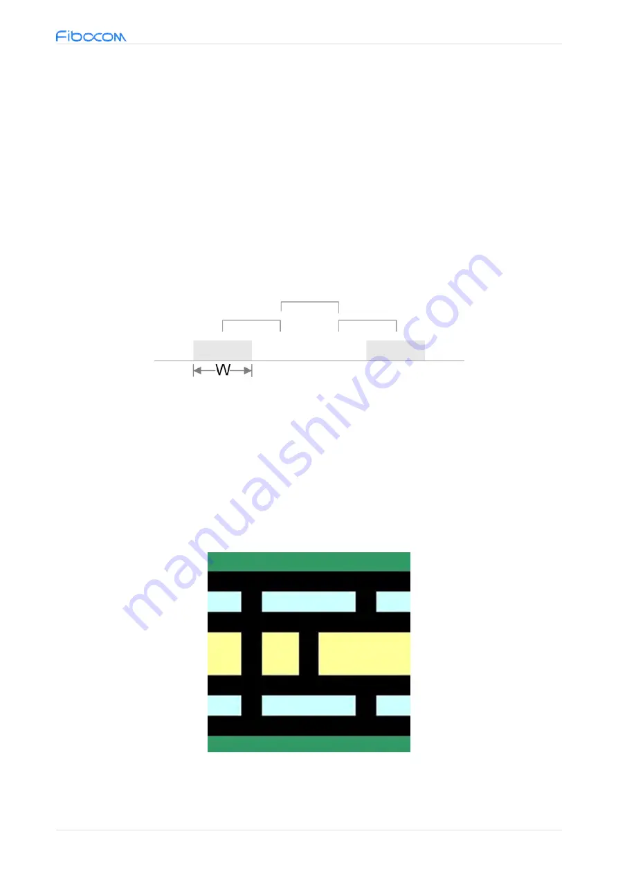
6.7.3. 3W Principle
During antenna RF signal cabling design on PCB, the first thing you need to consider is to
follow "3W principle".
In order to reduce crosstalk between the lines, please ensure that line spacing is large
enough. If the line spacing is at least 3 times of the line width, 70% of the electric field
between the lines will not interfere with each other, and this is called "3W principle".
Figure 21. 3W principle
6.7.4. Impedance Design for Four-layer Board
The thickness of four-layer board is 1.0 mm. RF line is routed on Lay 1, and reference
layer is on Lay 2 (GND layer).
The stacking varies with PCB vendor, the following figure is taken as an example.
Figure 22. Four layers (1+2+1) thickness
6. Radio Frequency
Copyright © Fibocom Wireless Inc.
51
Fibocom Confidential

