Reproduction forbidden without Fibocom Wireless Inc. written authorization - All Rights Reserved.
L830-EB-11 Hardware User Manual
Page 17 of 39
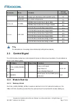
Parameter
Mode
Condition
Average
Current(mA)
LTE FDD
Paging cycle #64 frames (0.64 sec DRX cycle)
3.6
Radio Off
AT+CFUN=4,Flight mode
1.0
I
WCDMA-RMS
WCDMA
WCDMA Data transfer Band I @+23.5dBm
687
WCDMA Data transfer Band VIII @+23.5dBm
597
I
LTE-RMS
LTE FDD
LTE FDD Data transfer Band 1 @+23dBm
713
LTE FDD Data transfer Band 3 @+23dBm
733
LTE FDD Data transfer Band 7 @+23dBm
735
LTE FDD Data transfer Band 8 @+23dBm
675
LTE FDD Data transfer Band 20 @+23dBm
685
LTE FDD Data transfer Band 28 @+23dBm
833
Note
:
The data above is an average value obtained by testing some samples.
3.3
Control Signal
The L830 module provides two control signals for power on/off and reset operations, the pin defined as
shown in the following table:
Pin Pin Name
I/O
Reset Value Functions
Type
6
FULL_CARD_POWER_
OFF#
I
Power on/off signal
High: Power on
Low or floating: Power off
3.3V/1.8V
67
RESET#
I
Reset signal, internal 100KΩ pull-up,
active low.
1.8V
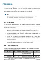
3.3.1 Module Start-Up
3.3.1.1 Start-up Circuit
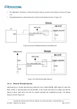
The FULL_CARD_POWER_OFF# pin needs an external 3.3V or 1.8V pull up for booting up. The
VDD(3.3V/1.8V) should be provided from the external circuit. Two methods for module starting up:


