background image


Reproduction forbidden without Fibocom Wireless Inc. written authorization - All Rights Reserved. 

FIBOCOM NL668-LA Series Hardware Guide   


  Page 22 of 61 

Table 4-2 Filter capacitors design of power supply 

Recommended Capacitor 

Application 

Description 

220uF x 2 

Regulating capacitor 

Reduce power fluctuations during 

module operation, requiring low ESR 

Capacitor 

LDO or DCDC power requires not 

less than 440uF capacitor 

Battery power can be properly 

reduced to 100uF ~ 220uF capacitor 

1uF, 100nF 

Digital signal noise 

Filter clock and digital signal 

interference 

39pF, 33pF 

700, 850/900 MHz bands 

Filter low band RF interference 

18pF, 8.2pF, 6.8pF 

1700/1800/1900,2100/2300,2500/

2600MHz bands 

Filter middle/high band RF 

interference 


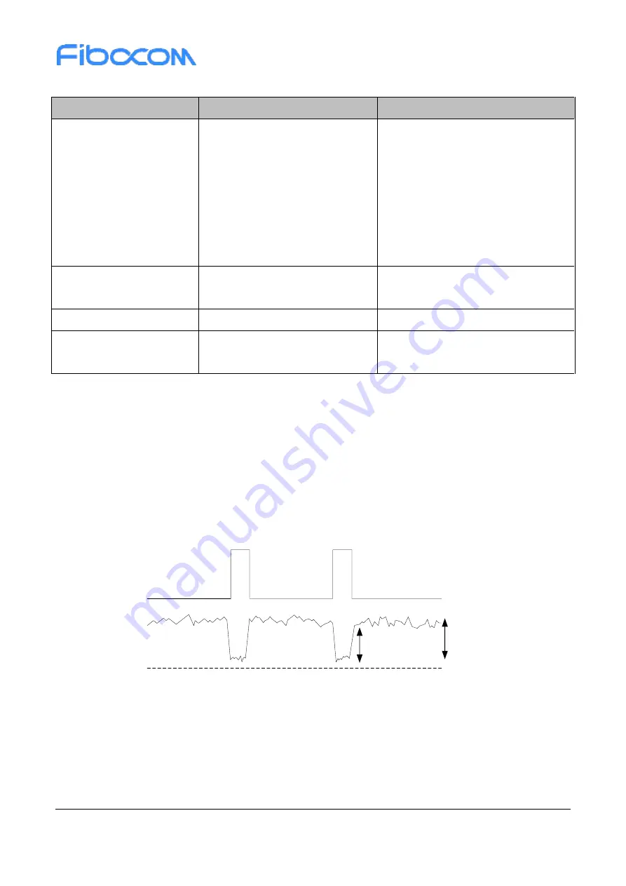
The power stability can ensure the normal operation of NL668-LA module. The power supply ripple limit 

for the module is no more than 300mV (the circuit ESR < 100mΩ) requires special attention when design 

circuit. 

When the module is operating in GSM mode (Burst transmit), the maximum operating current can reach 

3A, and the power voltage needs to be at least 3.3V. Otherwise, the module may power off or restart. The 

power limit is shown in Figure 4-2: 

Burst transmit

Burst transmit

min:3.3V

VBAT

Ripple

300mV

Drop 

VBAT

3.3V


Figure 4-2 Power limit


4.3 1.8V Output 

The NL668-LA series module outputs a 1.8V voltage through the VDD_EXT for the use of the internal 

digital circuit of module. The voltage is the logic level of the module and can be used to indicate module 

Summary of Contents for NL668-LA

Page 1: ...ction forbidden without Fibocom Wireless Inc written authorization All Rights Reserved FIBOCOM NL668 LA Series Hardware Guide Page 1 of 61 FIBOCOM NL668 LA Series Hardware Guide Version V1 0 9 Date 2022 03 29 ...

Page 2: ...t Fibocom Wireless Inc written authorization All Rights Reserved FIBOCOM NL668 LA Series Hardware Guide Page 2 of 61 Applicability Type N o Product Model Description 7 NL668 LA MCP is 4Gbit Flash 2Gbit RAM support MAIN_ANT DIV_ANT ...

Page 3: ...dividual is prohibited to excerpt copy any part of or the entire document or transmit the document in any form Notice The document is subject to update from time to time owing to the product version upgrade or other reasons Unless otherwise specified the document only serves as the user guide All the statements information and suggestions contained in the document do not constitute any explicit or...

Page 4: ...del NL668 LA 30 40 V1 0 7 Guo Zhenqi Tan Lefan Jin Haibo 2021 05 10 Modify pin 138 refer to design description V1 0 6 Tan Lefan Hu Wenkai Luke Liu 2021 03 10 Add model NL668 LA 05 and NL668 LA 10 V1 0 5 Lee Du Hu Wenkai Luke Liu 2020 08 10 Update product appearance V1 0 4 Hu Wenkai Lee Du Luke Liu 2020 03 13 Update power consumption V1 0 3 Lee Du Hu Wenkai Luke Liu 2020 01 10 Add model NL668 LA 01...

Page 5: ...Function 13 4 Electrical Characteristics 21 4 1 Power 21 4 2 Power Supply 21 4 3 1 8V Output 22 4 4 Power Consumption 23 5 Functional Interface 25 5 1 Control Interface 25 5 1 1 Power On Off 25 5 1 1 1 Power On 25 5 1 1 2 Power Off 26 5 1 2 RESET 27 5 2 Network Status Indicate Interface 29 5 2 1 Interface Status Description 29 5 3 U SIM Card Interface 30 5 3 1 U SIM Pin Definition 30 5 3 2 U SIM I...

Page 6: ... 40 6 2 1 USB Application Nonsupport USB Suspend Support VBUS 40 6 2 2 USB Application Nonsupport USB Suspend Nonsupport VBUS 41 6 2 3 USB Application Support USB Suspend 41 6 2 4 UART Application WAKEUP_IN Pin Level Control 41 6 2 5 UART Application DTR Pin Level Control 42 6 2 6 ATS24 Command 42 7 RF Interface 44 7 1 Operating Bands 44 7 2 Output Power 44 7 3 Receive Sensitivity 45 7 4 GNSS Rece...

Page 7: ...7 of 61 8 3 Environmental Reliability Requirements 51 8 4 ESD Characteristics 51 9 Structure Specification 53 9 1 Product Appearance 53 9 2 Structure Dimension 53 9 3 PCB Soldering Pad and Stencil Design 54 9 4 SMT 54 9 5 Carrier and storage 54 10 Regulatory 55 11 Terms and Acronyms 59 11 1 Related Documents 60 11 2 Reference Standards 61 ...

Page 8: ...ou drive do not use the handheld devices even if it has a hand free feature Please stop and call Please turn off the mobile device before boarding The wireless feature of the mobile device is not allowed on the aircraft to prevent interference with the aircraft communication system Ignoring this note may result in flight safety issue or even breaking the law When in a hospital or health care facil...

Page 9: ...OCOM NL668 LA Series Hardware Guide Page 9 of 61 Keep the mobile device away from flammable gases Turn off the mobile device when near gas stations oil depots chemical plants or explosive workplaces There is a safety hazard in operating electronic equipment in any potentially explosive environment ...

Page 10: ... 1 2 3 4 5 7 8 20 28 WCDMA HSPA Band 1 2 5 8 Data transmission LTE FDD Rel 9 150Mbps DL 50Mbps UL Cat 4 LTE Downlink MIMO 2 2 4 2 support part of R10 WCDMA Rel 8 UMTS 384 kbps DL 384 kbps UL DC HSDPA 42MbpsDL Cat24 HSUPA 5 76Mbps UL Cat 6 Power 3 3V to 4 3V typical 3 8V Temperature Normal 30 C to 75 C Extended 40 C to 85 C 1 Storage 40 C to 90 C Power consumption Base current 2mA Sleep mode 4mA Id...

Page 11: ... Text and PDU modes Note 1 When the temperature is beyond the normal operating temperature range 30 C to 75 C the RF performance of the module may slightly exceed the 3GPP specification 2 Models with Memory configured as 1Gbit Flash 1Gbit RAM are optional and available in two versions Data version supports DFOTA upgrade voice version does not support DFOTA upgrade 3 The data version does not suppo...

Page 12: ...e Page 12 of 61 2 4 Evaluation Board Fibocom provides EVK GT8230 NL ADP NL668 LA EVB LGA F01 ADP NL668 CN 30 00 development board to facilitate module debugging and use Note Nl668 LA 05 10 30 31 40 models use EVB LGA F01 ADP NL668 CN 30 00 development board Nl668 LA 00 01 models use the EVK GT8230 NL ADP NL668 LA development board ...

Page 13: ...es module is available in 144 pins The numbers of the LCC pins are 80 and the LGA pins are 64 the top view of the pin assignment is shown as follow figure Figure 3 1 Pin assignment top view diagram 85 to 112 are thermal pins and the module is grounded internally It is recommended that the heat sink pad is reserved for PCB packaging and welded 3 2 Pin Function Table 3 1 I O description parameters N...

Page 14: ...IHmin 1 2V VIHmax 2 0V External device wake up module low active by default with software programmable option Boot_config GPIO forbidden to pull up externally 2 AP_READY I VILmin 0 3V VILmax 0 6V VIHmin 1 2V VIHmax 2 0V Reserved 3 RESERVED Reserved 4 W_DISABLE I VILmin 0 3V VILmax 0 6V VIHmin 1 2V VIHmax 2 0V Module flight mode control pull up by default Pull down this pin module enter airplane mo...
Page 15: ...ax 0 6V VIHmin 1 2V VIHmax 2 0V U SIM card hot plug detection 14 USIM_VDD PO For 1 8V U SIM Vmax 1 9V Vmin 1 7V For 3 0V U SIM Vmax 3 05V Vmin 2 7V IOmax 50mA U SIM power identify 1 8V or 3V U SIM card automatically 15 USIM_DATA IO For 1 8V U SIM VILmax 0 6V VIHmin 1 2V VOLmax 0 45V VOHmin 1 35V For 3 0V U SIM VILmax 1 0V VIHmin 1 95V VOLmax 0 45V VOHmin 2 55V U SIM data signal 16 USIM_CLK O For 1...

Page 16: ...y The input is pulled up to an internal voltage minus a diode drop As per the design this causes the voltage of the pin is about 0 8V 22 GND G Ground 23 SD_INS_DET I Reserved 24 PCM_IN I VILmin 0 3V VILmax 0 6V VIHmin 1 2V VIHmax 2 0V PCM input signal 25 PCM_OUT O VOLmax 0 45V VOHmin 1 35V PCM output signal 26 PCM_SYNC IO VOLmax 0 45V VOHmin 1 35V VILmin 0 3V VILmax 0 6V VIHmin 1 2V VIHmax 2 0V PC...

Page 17: ..._SDA OD I2C interface data signal 43 NC NC 44 ADC1 I Analog to digital converter interface1 45 ADC0 I Analog to digital converter interface 0 46 GND G Ground 47 ANT_GNSS I GNSS antenna 48 GND Ground 49 ANT_MAIN IO Main antenna 50 GND G Ground 51 GND G Ground 52 GND G Ground 53 GND G Ground 54 GND G Ground 55 NC NC 56 GND G Ground 57 VBAT_RF PI Vmax 4 3V Vmin 3 3V Vnorm 3 8V RF power input 3 3V 4 3...

Page 18: ... 35V Request to send 65 RTS I VILmin 0 3V VILmax 0 6V VIHmin 1 2V VIHmax 2 0V Clear to send 66 DTR I VILmin 0 3V VILmax 0 6V VIHmin 1 2V VIHmax 2 0V Data ready The control of the sleep mode 67 TXD O VOLmax 0 45V VOHmin 1 35V Transmit data 68 RXD I VILmin 0 3V VILmax 0 6V VIHmin 1 2V VIHmax 2 0V Receive data 69 USB_DP IO Conform to USB2 0 standard specification USB differential data bus 70 USB_DM I...

Page 19: ... I Reserved 121 SGMII_MDATA IO Reserved 122 SGMII_MCLK O Reserved 123 SGMII_TX_M O Reserved 124 SGMII_TX_P O Reserved 125 SGMII_RX_P I Reserved 126 SGMII_RX_M I Reserved 127 PM_ENABLE O Reserved 128 VREG_L5_UIM2 PO Reserved 129 SDC1_DATA3 IO Reserved 130 SDC1_DATA2 IO Reserved 131 SDC1_DATA1 IO Reserved 132 SDC1_DATA0 IO Reserved 133 SDC1_CLK O Reserved 134 SDC1_CMD O Reserved 135 WAKE_WLAN I Rese...

Page 20: ...tion forbidden without Fibocom Wireless Inc written authorization All Rights Reserved FIBOCOM NL668 LA Series Hardware Guide Page 20 of 61 Note Keep the unused pins floating The reserved pins are in development ...

Page 21: ...ion VBAT_RF PI 57 58 Module power supply 3 3V 4 3V typical value 3 8V VBAT_BB PI 59 60 Module power supply 3 3V 4 3V typical value 3 8V VDD_EXT PO 7 Module digital voltage output 1 8V 80mA GND G 8 9 10 19 22 36 46 48 50 54 56 72 76 85 112 All GND pins must be grounded Note In the rest of the document VBAT includes VBAT_BB and VBAT_RF 4 2 Power Supply The NL668 LA series module needs to be powered ...

Page 22: ...0 1800 1900 2100 2300 2500 2600MHz bands Filter middle high band RF interference The power stability can ensure the normal operation of NL668 LA module The power supply ripple limit for the module is no more than 300mV the circuit ESR 100mΩ requires special attention when design circuit When the module is operating in GSM mode Burst transmit the maximum operating current can reach 3A and the power...

Page 23: ...e refer to 6 1 2 section Table 4 4 Power consumption Parameter Mode Condition Average Current Typ mA Ioff Power off Module power off 0 03 Iidle Radio off GSM MFRMS 5 USB sleep 20 MFRMS 5 USB wakeup 30 WCDMA DRX 8 USB sleep 20 DRX 8 USB wakeup 30 LTE FDD Paging cycle 64 frames USB sleep 20 Paging cycle 64 frames USB wakeup 30 LTE TDD Paging cycle 64 frames USB sleep 20 Paging cycle 64 frames USB wa...

Page 24: ...r Band 2 23 5dBm 620 WCDMA Data transfer Band 5 23 5dBm 550 WCDMA Data transfer Band VIII 23 5dBm 570 ILTE RMS LTE FDD LTE FDD Data transfer Band 1 23dBm 650 LTE FDD Data transfer Band 2 23dBm 650 LTE FDD Data transfer Band 3 23dBm 730 LTE FDD Data transfer Band 4 23dBm 700 LTE FDD Data transfer Band 5 23dBm 580 LTE FDD Data transfer Band 7 23dBm 750 LTE FDD Data transfer Band 8 23dBm 580 LTE FDD ...

Page 25: ... power off mode pull down PWRKEY 100ms to 2s and release it the module will power on When module in operating mode pull down PWRKEY 3s to 8s and then release it the module will power off 5 1 1 Power On Off 5 1 1 1 Power On When NL668 LA series module in power off mode pull down PWRKEY pin 100ms to 2s the module will power on it is recommended to use OC OD drive circuit to control PWRKEY pin The OC...

Page 26: ...f 61 Figure 5 2 Button switch power on reference circuit Figure 5 3 shows power on timing Figure 5 3 Power on timing Note Before pull down PWRKEY pin the Voltage of VBAT must be stable recommended time interval between VBAT enable and pull down PWRKEY pin at least 30ms 5 1 1 2 Power Off The module supports three power off methods as table 5 2 ...

Page 27: ...off AT power off AT CPWROFF Software normal power off Note 1 When module at operating mode please do not cut off module power supply to avoid damage internal flash Recommended by PWRKEY pin or AT commands power off module then cut off power supply 2 When power off by AT commands please don t pull down PWRKEY pin otherwise module will power on again automatically The power off timing is shown as fo...

Page 28: ...ardware Guide Page 28 of 61 Clients can control RESET_N pin by two modes OC OD drive circuits and button switch corresponding reference circuit as Figure 5 5 and Figure 5 6 Figure 5 5 OC driven reset reference circuit Figure 5 6 Button reset reference circuit The reset timing is shown as follows Figure 5 7 Reset timing ...

Page 29: ...status indicator 5 2 1 Interface Status Description Network status indicate pins are used to driven indicate light and describe module s network status NL668 LA series module network indicates light work status description as follow table Table 5 5 Network indicator light work status Mode Module Network Indicator Pin Status Indicator Light Flash Off Status Description 1 600ms High 600ms Low Flash ...

Page 30: ...Pin Definition U SIM pin definition is shown in the following table Table 5 6 U SIM card pin Pin name I O Pin No Description USIM_PRESENCE I 13 Detect U SIM card for Hot swap USIM_VDD PO 14 U SIM Power USIM_DATA IO 15 U SIM DATA USIM_CLK O 16 Clock Signal USIM_RESET O 17 Reset Signal 5 3 2 U SIM Interface Circuit 5 3 2 1 U SIM Card Connector with Card Detection Signal U SIM circuit design requires...

Page 31: ...1 of 61 Figure 5 9 U SIM card connector SIM016 8P 220P SIM016 8P 220P card connector DET and POL are short connected when the card is inserted DET and POL are disconnected when there is no card The following is the reference design circuit U SIM card insert USIM_PRESENCE pin is high level U SIM card pull out USIM_PRESENCE pin is low level ...

Page 32: ...d connector without detection signal USIM_ PRESENCE pin must keep floating Figure 5 11 U SIM card connector without detection signal reference circuit 5 3 3 U SIM Hot Plug NL668 LA series module support U SIM hot plug function it determines the insertion and removal of U SIM card by detect the USIM_ PRESENCE pin state The card hot plug function can be configured by the AT MSMPD command and the AT ...

Page 33: ...the USIM_PRESENCE is in low level the module detects U SIM card is removed and it will not read the U SIM card Note The USIM_PRESENCE pin active high by default and can be switched to active low by AT command Table 5 8 USIM_PRESENCE effective level switched AT Command Function Description AT GTSET SIMPHASE 1 Default high level detect AT GTSET SIMPHASE 0 Low level detect 5 3 4 U SIM Design Requirem...

Page 34: ...e 5 9 USB pin definition Pin name I O Pin No Description USB_DP IO 69 USB differential data bus D USB_DM IO 70 USB differential data bus D USB_VBUS PI 71 USB Plug detect For more information about the USB 2 0 specification please refer to http www usb org home Note Since the module supports USB 2 0 High Speed TVS tube equivalent capacitance on the USB_DM DP differential signal cable is required to...

Page 35: ...ebug Table 5 8 and table 5 9 are the pin definition of main serial port and debug serial port Table 5 10 Main serial port Pin Name I O Pin No Description RI O 62 Ring indicator DCD O 63 Data carrier detection CTS O 64 Request to send RTS I 65 Clear to send DTR I 66 Data ready sleep mode control TXD O 67 Module Transmit data RXD I 68 Module Receive data Table 5 11 Debug serial port Pin Name I O Pin...

Page 36: ... rest input and output circuit design of dotted line please refer to solid line part but pay attention to signal connection direction Figure 5 13 UART level translate reference 2 Note Level translate circuits is not suitable for applications of baud rates above 460Kbps 5 6 ADC Interface NL668 LA series module support two channels ADC interface Use AT MMAD command can read the value of ADC interfac...

Page 37: ...s module provides a PCM interface for communication with digital audio devices such as an external CODEC 5 7 1 Supported Model Table 5 13 Supported model of PCM Product model Description NL668 LA 00 Support NL668 LA 01 Support NL668 LA 05 Support NL668 LA 10 Support NL668 LA 30 Support NL668 LA 40 Support NL668 LA 31 Support 5 7 2 PCM Interface Definition Table 5 14 PCM pin definition Pin Name I O...

Page 38: ...as master PCM CLK PCM_OUT PCM Output PCM_IN PCM Input PCM_SYNC 8KHz Short pulse PCM Synchronous Signal Falling edge sampling NL668 LA series module adopts the above configuration by default any adjustment please contact Fibocom Wireless technical support 5 7 4 PCM Signal Description The PCM signal of NL668 LA series module adopts domestic mainstream Europe E1 standard PCM_CLK frequency is 2 048MHz...

Page 39: ...time 125 μs t synca PCM_SYNC asserted time 488 ns t syncd PCM_SYNC deasserted time 124 5 μs t clk PCM_CLK cycle time 488 ns t clkh PCM_CLK high time 244 ns t clkl PCM_CLK low time 244 ns t susync PCM_SYNC offset time to PCM_CLK falling 122 ns t sudin PCM_DIN setup time to PCM_CLK falling 60 ns t hdin PCM_DIN hold time after PCM_CLK falling 10 ns t pdout Delay from PCM_CLK rising to PCM_DOUT valid ...

Page 40: ... it down module enter airplane mode 2 AT command control AT CFUN 4 module enter airplane mode AT CFUN 1 module enter normal mode 6 2 Sleep Mode 6 2 1 USB Application Nonsupport USB Suspend Support VBUS If the host nonsupport USB suspend function the module can enter sleep mode by disconnect USB_VBUS from the external control circuit Sleep Send AT GTUSBDETECTEN 1 to enable USB plug detect function ...

Page 41: ...lug in USB cable or enable the USB HUB controller can wake up the module 6 2 3 USB Application Support USB Suspend If the host support USB Suspend Resume Setting USB sleep in Linux system Sleep Send AT GTLPMMODE 1 X command to set the WAKEUP_IN pin s level of control module enter sleep mode Reset module command effective X 0 WAKEUP_IN pin is high level module enter sleep mode X 1 WAKEUP_IN pin is ...

Page 42: ...pin is high level module enter sleep mode X 1 DTR pin is low level module enter sleep mode AT GTUSBSLEEPEN 2 X command to disable USB function X can be 0 or 1 AT CSCLK 1 command to enable sleep function Wake up The level of DTR pin contrary with that when the module enters sleep mode module allow be wake up X 0 DTR pin is low level wake up module X 1 DTR pin is high level wake up module 6 2 6 ATS2...

Page 43: ... of 61 overtime strictly but try to enter sleep mode If system don t support after overtime it will timekeeping automatically If you want to use the RI signal to represent the state of the module please refer to the AT GTWAKE command in FIBOCOM AT Commands _Sleep For more sleep command description please refer to FIBOCOM AT Commands _Sleep ...

Page 44: ... bands Operating Band Description Mode Tx MHz Rx MHz Band 1 IMT 2100MHz LTE FDD WCDMA 1920 1980 2110 2170 Band 2 IMT 1900 LTE FDD WCDMA GSM 1850 1910 1930 1990 Band 3 DCS 1800MHz LTE FDD WCDMA GSM 1710 1785 1805 1880 Band 4 IMT 2100 LTE FDD WCDMA 1710 1755 2110 2155 Band 5 CLR 850MHz LTE FDD WCDMA GSM 824 849 869 894 Band 7 IMT 2600 LTE FDD 2500 2570 2620 2690 Band 8 E GSM 900MHz LTE FDD WCDMA GSM...

Page 45: ...width 1 RB Band 5 23 2 10MHz Bandwidth 1 RB Band 7 23 2 10MHz Bandwidth 1 RB Band 8 23 2 10MHz Bandwidth 1 RB Band 20 23 2 10MHz Bandwidth 1 RB Band 28 23 2 10MHz Bandwidth 1 RB 7 3 Receive Sensitivity Table 7 4 Receive sensitivity Mode Band Rx Sensitivity dBm Typ RxD Sensitivity dBm Typ WCDMA Band1 109 110 Band2 109 5 110 5 Band5 110 110 5 Band8 110 110 5 LTE FDD Band 1 97 5 98 Band 2 97 5 98 5 B...

Page 46: ...N0 GNSS Signal 130dBm 38 5 dB Hz Positional accuracy CEP GNSS Signal 130dBm 3 5m 7 4 2 GNSS Observe Protocol NL668 LA series module adopts NMEA 0183 protocol 7 5 Antenna Design 7 5 1 Antenna Index 1 Antenna efficiency Antenna efficiency is the ratio of antenna input power to radiated power Due to the antenna return loss material loss and coupling loss the radiated power is always lower than the in...

Page 47: ...gth of electromagnetic wave in all directions Gain is a collection of antenna benefits and antenna directivity 6 Interference In addition to the antenna performance other interferences on the PCB also affect the performance of the module In order to ensure the high performance of the module interference must be controlled Suggestions For example LCD CPU FPC cable audio circuit power supply should ...

Page 48: ...dBm average power WCDMA LTE TD SCDMA CDMA EVDO Standing wave ratio recommended 2 1 7 5 2 Antenna Reference Design Antenna is a sensitive device susceptible to the external environment For example the size of the module the location of the antenna the space it occupies and the surrounding ground all may affect antenna performance In addition the RF cable connect with antenna and the location of the...

Page 49: ...stic impedance of transmission cable is 50 ohms Since the antenna loss should be less than 0 3dB keep PCB cable as short as possible Keep the PCB LAYOUT straight and reduce holes on the route to another layer also avoid right angle and acute angle wiring PCB cable should have a good reference ground to avoid other signal cable near the antenna Recommend a complete ground level and use this complet...

Page 50: ...tage 0 3 1 8 2 0 V 8 1 2 Operating Voltage Range Table 8 2 Operating Voltage Range Parameter VL VH Unit Min Max Min Max Digital input 0 3 0 6 1 2 2 0 V Digital output 0 45 1 35 V VL logic low level VH logic high level Parameter I O Min Typ Max Unit VBAT PI 3 3 3 8 4 3 V USIM_VDD PO 1 7 2 75 1 8 2 85 1 9 2 95 V 8 2 Environment Temperature Range The recommended operating temperature range of NL668 L...

Page 51: ...w temperature operating test Temperature 30 3 24 hours in operating state High temperature operating test Temperature 75 3 24 hours in operating state Vibration test When the frequency is 5Hz to 20Hz the random vibration ASD Acceleration Spectral Density is 0 96m2 s3 When the frequency is 20Hz to 500Hz the random vibration ASD is 0 96 m2 S3 20Hz For other frequencies the random vibration ASD is 3d...

Page 52: ...n without Fibocom Wireless Inc written authorization All Rights Reserved FIBOCOM NL668 LA Series Hardware Guide Page 52 of 61 Interface Air Discharge Contact Discharge GND 10KV 5KV Antenna port 8KV 4KV Other port 1KV 0 5KV ...

Page 53: ...s Hardware Guide Page 53 of 61 9 Structure Specification 9 1 Product Appearance The product appearance of NL668 LA series module is shown in Figure 9 1 Figure 9 1 Product appearance 9 2 Structure Dimension The structure dimension of NL668 LA series module is shown as Figure 9 2 Figure 9 2 Structure dimension unit mm ...

Page 54: ... 61 9 3 PCB Soldering Pad and Stencil Design PCB soldering pad and stencil design please refer to FIBOCOM NL668 LCC SMT Design Guide 9 4 SMT SMT production process parameters and related requirements please refer to FIBOCOM NL668 LCC SMT Design Guide 9 5 Carrier and storage Carrier and storage please refer to FIBOCOM NL668 LCC SMT Design Guide ...

Page 55: ...ed FIBOCOM NL668 LA Series Hardware Guide Page 55 of 61 10 Regulatory CE Conformance information The device could be used with a separation distance of 20cm to the human body Hereby Fibocom Wireless Inc declares that the radio equipment type NL668 LA is in compliance with Directive 2014 53 EU ...

Page 56: ...ssions are complaint with the transmitter s rule s The Grantee will provide guidance to the host manufacturer for Part 15 B requirements if needed Important Note notice that any deviation s from the defined parameters of the antenna trace as described by the instructions require that the host product manufacturer must notify to Fibocom wires Inc that they wish to change the antenna trace design In...

Page 57: ...e and 2 this device must accept any interference received including interference that may cause undesired operation This equipment has been tested and found to comply with the limits for a Class B digital device pursuant to Part 15 of the FCC Rules These limits are designed to provide reasonable protection against harmful interference in a residential installation This equipment generates uses and...

Page 58: ...en the grantee shall provide a notice stating that the final host product still requires Part 15 Subpart B compliance testing with the modular transmitter installed This device is intended only for OEM integrators under the following conditions For module device use 1 The antenna must be installed such that 20 cm is maintained between the antenna and users and 2 The transmitter module may not be c...

Page 59: ...l System for Mobile Communications HSDPA High Speed Down Link Packet Access IMEI International Mobile Equipment Identity Imax Maximum Load Current LED Light Emitting Diode LSB Least Significant Bit LTE Long Term Evolution CA Carrier Aggregation DLCA Downlink Carrier Aggregation SCell Secondary Cell for CA ME Mobile Equipment MS Mobile Station MT Mobile Terminated PCB Printed Circuit Board PDU Prot...

Page 60: ...e Value Vmin Minimum Voltage Value VIHmax Maximum Input High Level Voltage Value VIHmin Minimum Input High Level Voltage Value VILmax Maximum Input Low Level Voltage Value VILmin Minimum Input Low Level Voltage Value VImax Absolute Maximum Input Voltage Value VImin Absolute Minimum Input Voltage Value VOHmax Maximum Output High Level Voltage Value VOHmin Minimum Output High Level Voltage Value VOL...

Page 61: ... V10 6 0 User Equipment UE conformance specification Radio transmission and reception Part 1 Conformance testing 3GPP TS 21 111 V10 0 0 USIM and IC card requirements 3GPP TS 51 011 V4 15 0 Specification of the Subscriber Identity Module Mobile Equipment SIM ME interface 3GPP TS 31 102 V10 11 0 Characteristics of the Universal Subscriber Identity Module USIM application 3GPP TS 31 11 V10 16 0 Unive...

Reviews: