Reproduction forbidden without Fibocom Wireless Inc. written authorization - All Rights Reserved.
FIBOCOM_NL952-NA_Hardware_User_Manual
Page 25 of 57
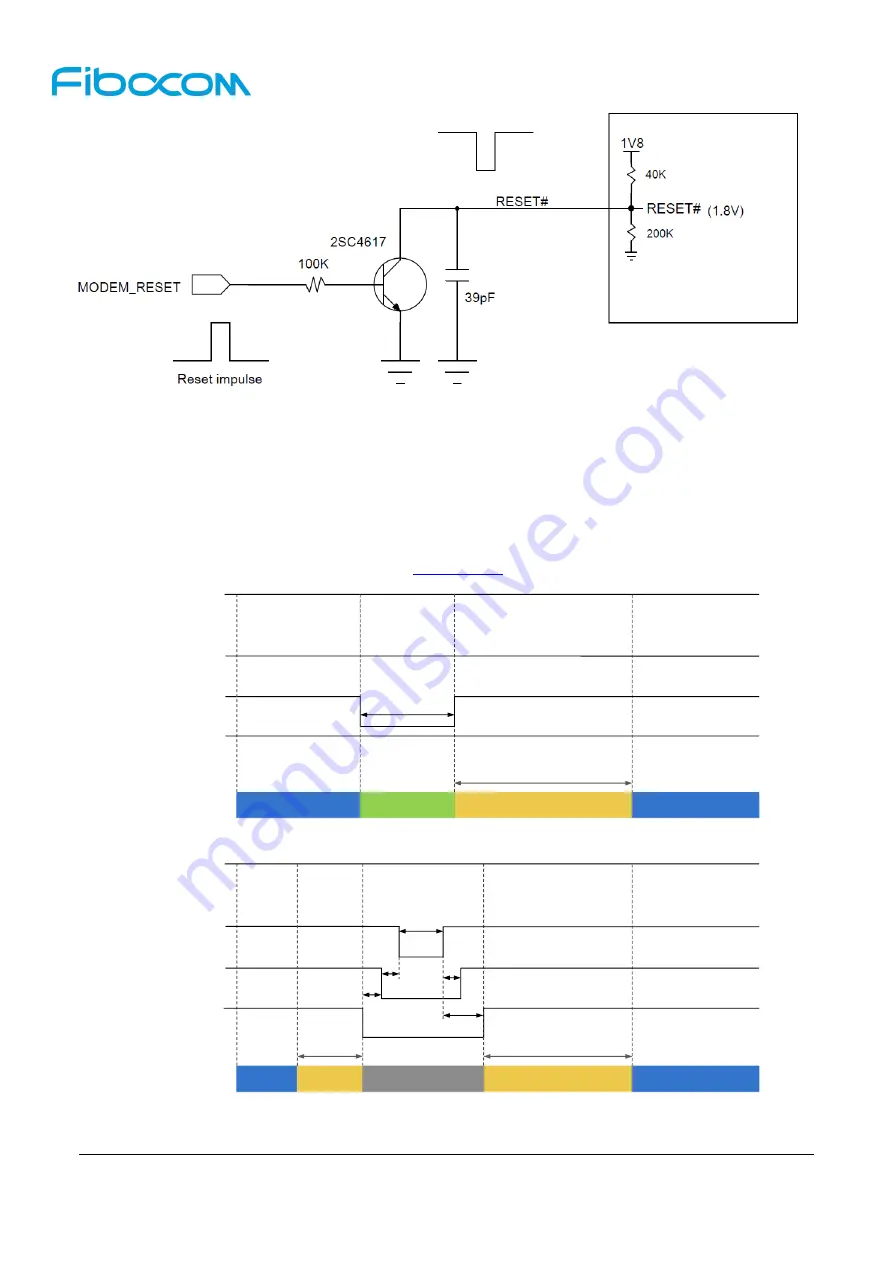
Figure 3-7 Recommended Design for Reset Circuit
There are two reset control timings as below:
Reset timing 1
st
in Figure 3-8, PMU of module internal always on in reset sequence, recommend
using in FW upgrade and module recovery;
Reset timing 2
nd
in Figure 3-9, PMU of module internal will be off in reset sequence (including whole
power off and power on sequence, t
sd
can refer
), recommend using in system warm boot.
+3.3V
PERST#
RESET#
Module State
Initialization
Activation
FCPO#
typical 20s
Baseband reset
Activation
t
off2
Figure 3-8 Reset control timing1
st
+3.3V
PERST#
RESET#
Module State
Initialization
Activation
FCPO#
typical 20s
Activation
t
off
Finalization
OFF
AT+CFUN=0
t
off2
t
off1
t
on1
t
on2
t
sd
Figure 3-9 Reset control timing2
nd


