Reproduction forbidden without Fibocom Wireless Inc. written authorization - All Rights Reserved.
FIBOCOM SU806 Series Hardware Guide
Page 29 of 91
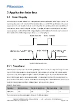
VRTC input voltage
-
3.0
-
V
VRTC input current
-
40
-
uA
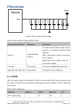
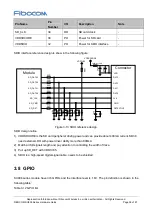
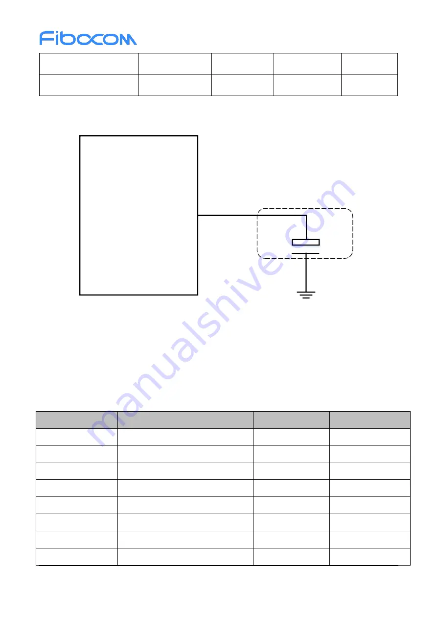
The reference design of VRTC pin powered by external power source is shown the following figure:
Module
VRTC
+
Coin cell
Figure 3-3 VRTC reference design
3.1.3 Power Output
The SU806 series module provides multiple power outputs for peripheral circuits. It is recommended to
connect 33pF and 10pF capacitors in parallel with every power to avoid high frequency interference
effectively.
Table 3-4 Power output
Pin Name
Programmable Voltage Range (V)
Default Voltage (V) Drive Current (mA)
VDD1V85
1.75-2.1
1.85
200
VDD1V8
1.10625-1.9
1.8
200
VDDCAMMOT
1.8-3.3
2.8
100
VDDSDCORE
1.8-3.3
3.0
400
VDDSDIO
1.8-3.3
3.0
100
VDDSIM0
1.8-3.3
1.8/3
50
VDDSIM1
1.8-3.3
1.8/3
50
VDDCAMA
1.8-3.3
2.8
150

