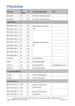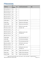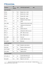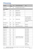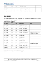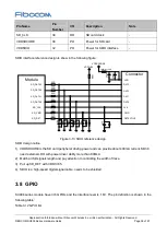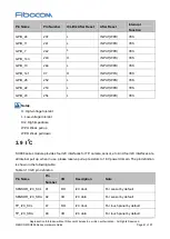
Reproduction forbidden without Fibocom Wireless Inc. written authorization - All Rights Reserved.
FIBOCOM SU806 Series Hardware Guide
Page 34 of 91
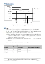
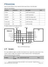
Connector
VBUS
DM
DP
ID
GND
Module
USB_DM
USB_DP
USB_ID
USB_VBUS
1
uF
VBAT
DC-DC
GPIO
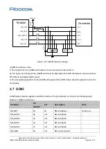
Figure 3-9 USB2.0 reference design (with OTG function)
Note:
1) Please choose junction capacitor less than 1pF for ESD protection device of USB_DP/DM
2) USB_DP and USB_DM are high-speed differential signal. The highest transmission rate is
480Mbps. Please pay attention to the following requirements in PCB layout:
USB_DP and USB_DM signal cables are required to be parallel and equal in length (differential
cable length controlled within 2mm), while the right-angle route shall be avoided, and
differential 90Ω impedance shall be controlled.
USB2.0 differential signal cable laid on the signal layer nearest to the ground, with well
grounded.
3) Please choose DC-DC that satisfy output is 5V when support OTG function.
Table 3-7 Length of USB differential signal line in module
Pin Name
Pin
Number
Length (mm)
Length Difference (DP-DM) mm
USB_DP
14
11.33134
0.40037
USB_DM
13
10.93097


