background image

Summary of Contents for 4265A

Page 1: ...If lukei Instruction Manual Vali tionics International Inc 00 0258 Wrtwl Ek COPY Model 4265A Binary Programmable Power Source P N 310631 JANUARY 1973 REV 1 2 76...

Page 2: ...THE DATE OF PURCHASE THE FOREGOING WARRANTY ISI INI LIEU OF ALL OTHER WARRANTIES EXPRESS OR IMPLIED INCLUDING BUT NOT LIMITED TO ANY IMPLIED WARRANTY OF MERCHANTABILITY FITNESS OR ADEQUACY FOR ANY PAR...

Page 3: ...ck Installation 2 1 2 10 Operating Features 2 3 2 12 Operating Notes 2 3 2 24 Programming Information 24 3 THEORY OF OPERATION 3 1 3 1 Introduction 3 1 3 3 Fundamental Circuit Description 3 1 3 5 Bloc...

Page 4: ...Isolated Logic Schematic Diagram 4200 1024 2 sheets Schematic Diagram 4200 1025 Rack Mounting Fixtures Program Connector Extender PCB assembly and Cable Extender Assembly 7 GENERAL INFORMATION 8 SCHE...

Page 5: ...1 Knowing that there is a problem 2 Learning the guidelines for handling them 3 Using the procedures and packaging and bench techniques that are recommended The Static Sensitive S S devices are ident...

Page 6: ...YPE SOLDER SUCKERS SHOULD BE USED 10 ONLY GROUNDED TIP SOLDERING IRONS SHOULD BE USED Anti static bags for storing S S devices or pcbs with these devices on them can be ordered from the John Fluke Mfg...

Page 7: ...e actual output is four times the programmed level Two s complement cod ing is required for negative outputs when the Isolated Con trol Logic 01 Option is installed All programming in puts and flag ou...

Page 8: ...r Available The Direct Coupled Control Logic is no longer offered as an option to the 4200 series instruments The Isolated Control Logic see descrip tion above is now standard equipment on alt instrum...

Page 9: ...0 10 E out Overload protected The Current Limit Flag is energized when a current sink overload condition occurs 0 01 of program 100 uV 0 01 of program 300 uV 500 uV rms 7mV pp 1 mV rms 7mV p p 0 02 mi...

Page 10: ...c 10 48 62 Hz single phase 200 watts fully loaded ENVIRONMENTAL Temperature 0 C to 50 C operating 40 C to 75 C storage Relative Humidity 0 to 80 Shock 20g 1 1 millisecond half sine wave Vibration 4 5g...

Page 11: ...will follow any command data perturbations Logic 1 hold condition RANGE EXTERNAL REFERENCE Connector Pin 29 Logic 0 Low Voltage Range Logic 1 High Voltage Range Connector Pin 36 Logic 0 Internal DC Re...

Page 12: ......

Page 13: ...T gic Timing 04 Option 2 8 2 8 Accuracy Versus External Reference Frequency 2 9 2 9 AC External Reference Feedthrough Versus Frequency OV Output 2 10 2 10 AC External Reference Phase Shift Versus Fre...

Page 14: ...nel Display Option 5 10 No Display PCB Assembly 05 Option S l 1 Current Limit PCB Assembly 06 Option 5 12 Power Amplifier PCB Assembly Sheet 1 of 2 Sheet 2 of 2 ACCESSORY MODEL A4200 6 1 Model A4200 M...

Page 15: ...Programming Input Outputs 14 2 1 Programming Input Outputs 2 6 2 2 Binary and Two s Complement Coding 16V Range 2 6 3 1 Operating Voltages 3 3 4 1 Recommended Test Equipment 4 1 4 2 Binary and Two s...

Page 16: ......

Page 17: ...ber when requesting a new shipping container 2 6 INPUT POWER 2 7 This power source can be operated from either a 1 15 or 230 vac 48 to 62 Hz power line A decal on the rear panel indicates which power...

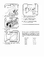
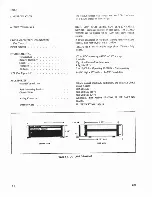
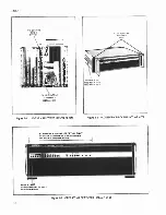
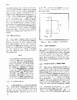
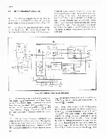
Page 18: ...4265A Figure 2 1 115 230 VAC POWER CONVERSION Figure 2 2 ACCESSORY RACK MOUNTING KITS...

Page 19: ...vides connection to chassis and earth ground See para 2 20 Figure 2 3 OPERATING FEATURES Sheet 2 of 2 cessories is given in the Section 6 Rack Installation sub section 2 10 OPERATING FEATURES 2 11 The...

Page 20: ...eads between the OUTPUT and SENSE terminals and the load must be large enough to carry the load current of up to 1 ampere and the sense cur rent of 1 ma without exceeding this voltage 2 20 Ground Conn...

Page 21: ...m med with binary coded inputs at pms 1 through 14 of the Programming Connector When the 16 volt range is called resolution is in 1 mv steps In the 65 volt range resolution is in 4 mv steps and the pr...

Page 22: ...RATE LOGIC 0 3 OPERATE 1 nmr 1 STANDBY 35 36 37 SIGN LOGIC 0 3 POSITIVE OUTPUT LOGIC 1 3 NEGATIVE OUTPUT EXTERNAL REFERENCE 03 Option LOGIC 0 INTERNAL REFERENCE LOGIC 1 3 EXTERNAL REFERENCE READY NOT...

Page 23: ...any program changes which is nor mal for direct programming The 100 Msec READY NOT READY FLAG begins at the end of positive transition of the DATA STROBE and serves to indicate the source has had time...

Page 24: ...xternal Reference 03 Option is in stalled a single programming bit is used to remove the inter nal 10 vdc reference from the D to A ladder network and switch in an external signal source to replace it...

Page 25: ...ld be noted that the rated output of the power sup ply is 66v minimum at l ampere Higher voltage output is obtainable depending on line voltage and output current i e 85v typical at 1 15 vac line and...

Page 26: ...4265A Figure 2 9 AC EXTERNAL REFERENCE FEED Figure 2 10 AC EXTERNAL REFERENCE PHASE THROUGH VERSUS FREQUENCY OV OUTPUT SHIFT VERSUS FREQUENCY Figure 2 11 AC EXTERNAL REFERENCE HAR MONIC DISTORTION VE...

Page 27: ...a gram that includes all options 3 3 FUNDAMENTAL CIRCUIT DESCRIPTION 34 The Model 4265A converts a digital program word into a representative dc output voltage Basically the cir cuitry consists of a h...

Page 28: ...Supply and the A 10 Connector Board Commands from the A6 Logic determine the polarity of VR p applied to VREp bus line A POL command produces a VRpp and a POL command a VR p Presence of either or both...

Page 29: ...etween 10 ma and l l ampere in 10 percent steps on two separate ranges In the event the output current is clamped at that level by action of the A8 Programmable Current Limiter During periods of curre...

Page 30: ...A9 Power Amplifier Diodes CRi through CR4 are connected as two full wave rectifiers to produce tVE operating 1 uge from the secondary of TL Cl and C2 1 liter the resulting outputs R1 and R2 function a...

Page 31: ...is provided by Q3 The differential Darlington composed of Q4 and Q5 amplifies the output of Ql and furnishes a single ended drive signal to Q7 This drive signal is de veloped across Q6 which functions...

Page 32: ...der resistor R 3 41 A6 Isolated Control Logic 4275A 1021 342 The A6 Isolated Control Logic assembly receives and processes all input and output data at the Programming Connector Jl A logic diagram m s...

Page 33: ...4265A STANDBY STROBE NOT READY FLAG CURRENT LIMIT FLAG 1 i 1 1 MHz OSCIL LATOR U19 ENABLE CURRENT LIMIT FLAG I F gure 3 5 ISOLATED CONTROL LOGIC Simplified 2 75 3 7Z3 8...

Page 34: ......

Page 35: ...de and external reference function is applied to the inputs of a series of multiplexing circuits as shown in Figure 3 5 When the data is settled at the multiplexer inputs the pro gram source generates...

Page 36: ...e power source NOTE Complementing magnitude data occurs only in binary type power sources 3 5 L COMPLEMENTING BINARY DATA 3 52 Binary type power sources require that negative values of magnitude data...

Page 37: ...d Q2 or Q3 respectively When an 8192 command 0V exists at terminal 18 of PI both Q4 and Q5 will be switched off Q3 is switched off by its resulting VA gate voltage and Ql Q2 are switched on by the res...

Page 38: ...mitter of Qll corresponds closely to the programmed output voltage A closed loop dc gain of five is established by feedback through R62 and R21 Overall frequency response is controlled to 6 db per oct...

Page 39: ...by definition Under this condition negative voltage more than 0 6V at the output will turn onCR25 which supplies base current for Q34 through R41 from common and adds to that supplied from the voltag...

Page 40: ...Q9 on the output voltage is 0 1 1 volt The range is set by R3 1 in parallel with R30 and is the 10 ina to 110 ma current range With Q26 turned off the range is deter mined by R30 alone This is the 10...

Page 41: ...a negligible effect in the OUTPUT LOW sense line 3 93 MINUS 16 VOLTS POWER SUPPLY Diode CR2 a 16 volt zener produces 16 volts at test point 4 This voltage is used in the Ground Isolator the FET Driver...

Page 42: ......

Page 43: ...repair work is done on an instrument that is beyond the warranty period 4 6 GENERAL MAINTENANCE 4 7 Cleaning 4 8 This power source should be cleaned periodically to remove dust grease or other contami...

Page 44: ...ocated on the A1 pcb The A1 and A7 pcb assemblies can then be sepa rated by removing the small screws on the A l pcb and then pulling the pcb assemblies apart NOTE A grounding jumper located adjacent...

Page 45: ...4265A Figure 4 1 ASSEMBLY ADJUSTMENT AND TEST POINT LOCATIONS TABLE 4 2 BINARY AND TWO S COMPLEMENT CODING 4 3...

Page 46: ...all 65V range and a 32 768V output 8192 bit g Adjust A2 A80 for a 32 768V dc 1 mV output h Call 65V range and a 16 384V output 4096 bit i Adjust A3 A4 for a 16 384V dc 1 mV output j Call 65V range and...

Page 47: ...b Adjust A3 ZERO for a 0V 10 uV output c Call 65V range and a 0V output The output should be 0V 30 uV If necessary adjust A3 ZERO until the specified results of step a through c are obtained d If the...

Page 48: ...uV 4096 2048 6 144V 300 uV 128 64 8 4 204 mV 40 uV 4096 2048 1024 7 168V 350 uV 256 16 1 273 mV 50 uV 8192 8 192V 400 uV 256 64 16 4 1 341 mV 50 uV 8192 1024 9 21 6V 450 uV 256 128 16 8 1 409 mV 50 uV...

Page 49: ...bassemblies of minor proportions are sometimes listed with the assembly of which they arc a part In this case the reference designations may appear out of order b The DESCRIPTION column describes the...

Page 50: ...Supply Codes is included in Appen dix A c The part number which uniquely identifies the item to the original manufacturer is listed in the MFG PART NO column If a component must be ordered by descript...

Page 51: ...modified during pro duction of the Model 4265A Each part for which a use code has been assigned may be identified with a particular instrument serial number by consulting the Use Code Effectivity List...

Page 52: ...5 10 Current Limit PCB Assembly 06 Option figure 5 11 Power Ampl PCB Assembly Figure 5 6 Figure 5 12 Connector PCB Assembly Figure 5 7 Figure 5 13 Connector programming male 50 contact Cover bottom C...

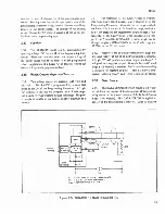
Page 53: ...4265A Figure 5 1 MODEL 4265A BINARY PROGRAMMABLE POWER SOURCE 5 5...

Page 54: ...4265A Figure 5 2 MOTHER PCB ASSEMBLY 5 6...

Page 55: ...ca 100 pf 5 500v Not used Cap cer 500 pf 10 l kv Cap elect 250 uf 50 10 64v Cap elect 2100 uf 50 10 150v Cap elect 8000 uf 100 10 15v Not used Cap Ta 1 0 uf 20 35v Cap cer 2000 pf gmv 1 kv Cap cer 0 1...

Page 56: ...4265A 4S V J H j 1 k Figure 5 3 POWER SUPPLY PCB ASSEMBLY 5 8...

Page 57: ...FET N channel Res comp lk 5 l 4w Res met flm 2 87k 1 l 8w Res met flm 17 4k 1 l 8w Res met flm 5 76k 1 l 8w Res met flm 13 7k 1 l 8w Res comp 22k 5 l 4w Res var cermet 2012 20 l 2w STOCK NO 285247 272...

Page 58: ...selected value may not be installed Res met flm 7 15k l l 8w Switch slide dpdt line voltage Switch toggle dpdt power Transformer power See Figure 5 1 IC operational amplifier 148064 202879 170720 1933...

Page 59: ...2 pf 5 500v CR1 CR2 CR5 CR6 Diode silicon 75 ma 90 piv CR3 CR4 CR7 thru CR12 Diode silicon 150 ma Q1 Q2 Q3 Q6 Q7 Q10 Q11 Q14 Q15 Q31 Q32 Tstr FET SET N channel Q4 Q8 Q12 Q16 Q34 Q37 Tstr silicon t PNP...

Page 60: ...4265A Figure 5 4 MODEL 4265A PRE AMPLIFIER PCB ASSEMBLY 5 12...

Page 61: ...l 2w R26 Res ww 25 01 3k 0 1 l 2w R27 Res ww 50k 0 1 l 2w R29 Res ww 100 025k 0 1 l 2w Matched Set 296095 1 R31 Res ww 200 075k 0 1 l 2w R35 Res ww 80 08k 0 1 l 2w R42 R43 Res ww r 13 328k 0 1 l 2w R2...

Page 62: ...8 Res met flm 10k 1 l 8w R71 Res comp 22k 5 l 4w R72 Res comp 10k 5 l 4w R73 R75 Res met flm 49 9k 1 l 2w R74 Res met flm 2 1k 1 l 2w R76 R80 Res comp 100ft 5 l 4w R77 R84 Res met flm I0k l l 2w R78 R...

Page 63: ...Q7 Q8 Tstr silicon NPN Q9 Q10 Tstr J FET N channel Qll Tstr silicon PNP QI3 Q14 Tstr silicon NPN R i Res ww 100 025k Matched Set R16 Res ww 99 955k R2 R1 1 Res comp lOfi 5 l 4w R3 R4 Res ww 6 8k 0 03...

Page 64: ...4265A A If r Figure 5 5 EXTERNAL REFERENCE PCB ASSEMBLY 03 EXTERNAL REFERENCE OPTION 5 16...

Page 65: ...5 1k 5 l 4w 193342 1 R23 R28 Res met flm 10k 1 l 2w 151274 2 R24 R29 Res met flm 4 87k 1 l 2w 247775 2 R25 Res met flm 2 49k 1 l 2w 193995 1 R26 Res comp lk 5 l 4w 148023 1 R27 R36 Res comp 82012 5 l...

Page 66: ...Q12 Q14 Q16 Q18 Q20 Q22 Q24 Q26 Q28 Q30 Q32 Q34 Q36 Q46 Q48 Q50 Q52 Not used Tstr silicon PNP Tstr J FET N channel U2366E Matched Pair Tstr J FET N channel U2366E Matched Pair Tstr J FET N channel U2...

Page 67: ...4265A Figure 5 6 BINARY LADDER PCB ASSEMBLY 5 19...

Page 68: ...0k 1 l 8w STOCK NO 289769 289777 29 1 088 290122 261701 29 1 054 EC USE TY CODE R24 R30 R36 R42 R48 R54 R60 R66R84 R90 R25 R27R28 R31 R33 R34 R37 R39 R40 R43 R45R46 R49 R51R52 R55 R57R58 R6l R63 R64 R...

Page 69: ...26 C42 Cap elect 200 rf 50 10 10V 236935 2 C27 Cap cer 2700 pf gmv 600V 106211 1 C30 Cap mica 620 pf 5 500V 215244 1 C31 C49 Cap mica 360 pf 1 500V 170407 2 C32 Cap mica 220 pf 5 500V 170423 1 C33 Cap...

Page 70: ...3 3k 5 l 4w Res met flm 6 98k 1 l 8w Res comp 5 112 5 l 4w Res met flm 10k 1 l 8w 267138 148189 193383 147975 234252 182956 193482 218032 148056 261685 221879 168260 I T1 thru T6 U1 U2 Not used Res m...

Page 71: ...os AND Gates IC TTL Quad 2 Input Nand Gate IC TTL Dual Peripheral Positive Nand Driver 293084 293092 292987 292953 329706 U15 U18 U20 U21 U22 IC TTL Monostable Multivibrator 1C TTL Retriggerable Monos...

Page 72: ...4265A Figure 5 7 ISOLATED CONTROL LOGIC 5 24 2 75...

Page 73: ...R72 R75 R78 R82 R83 U1 U2 U3 DIRECT COUPLED CONTROL LOGIC 04 OPTION Figure 5 8 Cap piste 01 uf 2 lOOv Cap elect 200 uf 50 10 lOv Diode zener S 6v Connector female 50 contact Tstr silicon NPN Res met...

Page 74: ...Jfc jft iM il 4265A LQGI C WON t ISOLATED i 1 Ln 5 26 Figure 5 8 NON ISOLATED LOGIC PCB ASSEMBLY 04 DIRECT COUPLED CONTROL OPTION 2 75...

Page 75: ...REF DESIG DESCRIPTION STOCK NO A7 CR1 thru CR27 R1 thru R27 U1 thru U5 DISPLAY BCD PCB ASSEMBLY Figure 5 8 Diode light emitting Res comp 27012 5 l 4w 1C TTL Hex Inverter 302257 309617 160804 292979...

Page 76: ...Jn AAA BOO OOP0 a m h lii OOO jTT t v Si Z i i n STTfJ J0L 1 35 OOOO M i f 4 t j V i P V C jjjk cl U l 3 4 i 33 ri 4y v W g BO W Hy Vi s 7 3 Figure 5 9 BINARY DISPLAY PCB ASSEMBLY 02 FRONT PANEL DISPL...

Page 77: ...4265A Figure 5 10 NO DISPLAY PCB ASSEMBLY 1 05 OPTION 5 29...

Page 78: ...v Cap piste 0 022 uf 10 250v Diode zener 16v Diode zener 3 9v 302331 175216 106062 190397 177998 106732 160317 234484 113332 CR4 CR8 CR6 CR9 Ql Q2 Q5 Q8 Q1 1 Q14 Ql 6 Q19 Q20 Q3 Q7 QIO Q13 Q15 Q21 Q23...

Page 79: ...4265A Figure 5 11 CURRENT LIMIT PCB ASSEMBLY 06 OPTION 5 31...

Page 80: ...50 R15 R54 R24 R25 R26 R35 R28 R34 R29 R53 R30 R52 R36 R49 R37 R48 R38 R46 R39 R47 R39 R47 R40 R45 Res comp 24k 5 l 4w Res comp I2k 5 l 4w Res comp 27k 5 l 4w Res met flm 6 19k 1 l 8w Res met flm 10k...

Page 81: ...1 U2 DESCRIPTION Res comp 1 2k 5 l 4w Res comp 100J2 5 l 4w Res ww 112 1 7c 2w Res met flm 1 2 4k i 1 l 8w Res comp 5612 5 l 4w 1C DTL Hex Inverter STOCK NO 190371 147926 229534 261644 147900 268367 E...

Page 82: ...50v 184366 C 1 2 C 14 C17 C18 C19 C20 Not used C23 Cap mica 150 pf 5 500v 148478 C24 C25 Cap piste 0 022 uf 10 250v 234484 C26 C27 Cap cer 0 01 uf 20 100v 149153 C28 C29 Cap mica 10 pf 10 500v 175216...

Page 83: ...9302 Rl R2 R9 RIO R23 Res comp 2k 5 l 4w 202879 R3 R8 R69 R73 Res comp 20k 5 l 4w 221614 R4 R6 Res comp 62k 5 l 4w 220053 R5 R7 Res comp 270tt 5 l 4w 160804 Rl 1 Res met flm 1 21k 1 l 8w 229146 Rl 2 R...

Page 84: ...mioc ass 4NV th3M0d 4265A Figure 5 12 POWER AMPLIFIER PCB ASSEMBLY Sheet 1 of 2 5 36...

Page 85: ...4265A Figure 5 12 POWER AMPLIFIER PCB ASSEMBLY Sheet 2 of 2 5 37...

Page 86: ...m 549ft 19c l 8w 289272 Res met flm 100ft 1 l 8w 168195 Res met flm 32 4k 1 l 8w 182956 Res comp I5k 5 l 4w 148114 Res comp 100k 5 l 4w 148189 Res comp 68 2 5 l 4w Res comp 1 2 5 l 2w Res comp 4 7k 10...

Page 87: ...4265A REF DESIG CRl thru CR4 Rl R2 DESCRIPTION CONNECTOR PCB ASSEMBLY Diode silicon i amp 600 piv Res comp 15k 10 2w STOCK NO...

Page 88: ...GB4721 HB 1531 TYPE R1250 IN4822 IN748 1N966A MST215N EB5105 CB1005 CB560S CB6805 CB 1 0 IS CB1825 CB3915 CB4715 CB5615 CB6815 CB8215 CB1025 CB152S CB3325 CB3925 CB4725 148106 01121 CB1035 1481 14 011...

Page 89: ...15 175042 01121 CB1825 193995 91637 TYPEMFF1 2 175216 01121 CD15C100K 194944 01121 CB1065 175224 14655 CD15E120J 195974 04713 2N3906 176644 14655 CD19F360G 202879 01121 CB2025 177980 14655 CD15F431J 2...

Page 90: ...901 01121 HB4721 91637 TYPE MFFl 8 89536 07910 01121 246173 TYPE 1N961B CB27G5 91637 TYPE MFF1 2 89536 254359 28480 5082 2900 89536 256487 91637 TYPE MFFl 8 91637 TYPE MFFl 8 360554 07910 CD55I05 2615...

Page 91: ...13 MC8308P 2884S0 91637 TYPE MFF1 8 293209 07263 U6B930959X 288845 01295 SN7402N 293761 91637 TYPE MFFl 8 2S92 2 91637 TYPE MFF 1 8 295212 71785 TYPE 140Y 289744 73445 C280CF A100K 296095 89536 296095...

Page 92: ...85 304808 89536 304808 306142 05397 3N173 306373 89536 306373 306381 89536 306381 306399 89536 306399 307017 02660 57 30500 3 308072 89536 308072 308122 89536 308122 309245 99392 61C15AS83 309302 3096...

Page 93: ...A4200 MCU is NOT compatible with the 09 option 6 4 In addition to providing signals to the voltage source the program source should also have the capability to receive status information from the volt...

Page 94: ...S 6 9 DATA WORD CONTROL WORD LENGTHS 6 10 BCD Type Voltage Sources 6 11 Program data for BCD type 4200 voltage sources consists of a 16 bit or a 18 bit data word and if necessary a control word up to...

Page 95: ...those voltage sources requiring range selection Logic 1 high range Logic 0 low range 31 55 External Reference Single line to program external reference mode on those voltage sources equipped with the...

Page 96: ...load the data word portion of the program data into the 4200 09 assembly Refer also to Dual Strobe Operation Either logic level may be used as selected by jumpers on PCB pads 22 23 and 24 9 12 Poll st...

Page 97: ...gram external reference mode on those voltage sources equipped with the external reference option Logic 1 ext reference Logic 0 int reference 2 28 Current limit range Single line to program range of c...

Page 98: ...also to Multi Strobe Operation Either logic level may be used as selected by jumpers on PCB pads 22 23 and 24 Single line used to poll status Vcc failure and current limit mode A logic 0 causes the g...

Page 99: ...ord see pads S T and U 6 21 14 to IS 16 to 17 H to F E to B D to C Polarity bit in 16 bit binary data word as last bit see Figure 6 5 6 21 17 to 14 H to G A to B Standby operate bit synchronous and po...

Page 100: ...ddress line enable positive 6 37 8 to 10 Mainframe address line enable negative 6 37 9 to 10 Data transferred by control word strobe 6 39 G to H D to E Data transferred by data word strobe 6 39 E to F...

Page 101: ...r 18 bits which make up the data word portion of the program data may be either positive true or negative true as determined by jumpering pads J K L M V and W For either logic polarity of BCD data pad...

Page 102: ...be commanded to the operate and standby modes by means of a unique standby operate line from the program source The standby operate command can be jumpered so that it is synchronous with the transfer...

Page 103: ...onger pulse which is issued by the program source after the control word and or data word has been applied to the parallel data inputs of the 4200 09 assembly In the single strobe mode the control wor...

Page 104: ...indicated by means of a the last 16th bit of the binary data word b a polarity bit as part of the control word 6 51 If the polarity is indicated in the last bit of the binary data word following the...

Page 105: ...50 2 49 3 48 47 5 46 6 45 21 NOTE In single strobe binary operation the mainframe address need only be present when transferring the control word When transferring the data wordr the power source whic...

Page 106: ...on for the polled power source does not exist However if the current limit flag bus responds with a ground level the current limit condition does exist and an overloaded power source is indicated 6 61...

Page 107: ...ogram data into shift registers which provide the necessary serial to parallel conversion The 4200 power sources require parallel program data The output of the hold one shot is present for the durati...

Page 108: ...4200 SERIES OPTION 09 Figure 6 8 4200 09 SIMPLIFIED BLOCK DIAGRAM 6 16 SHOT...

Page 109: ...ing transformers T3 and T5 at the guard shield On the inside of the guard shield the serial data and control words are loaded into a second set of shift registers which are clocked by the pulses at th...

Page 110: ...ready being generated during a data transfer sequence of 16 clock pulses As long as a data transfer sequence is not in progress the data transfer flip flop is in Us reset state When the data transfer...

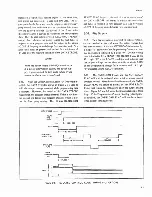
Page 111: ...SHIFT REGISTER SERIAL DAT 4200 SERIES OPTION 09 HOLD SIGNAL CURRENT LIMIT LAG 6 19 20...

Page 112: ......

Page 113: ......

Page 114: ...4200 SERIES OPTION 09 Table 6 5 TROUBLESHOOTING CHART INACTIVE PCB ASSEMBLY Sheet 1 of 2 6 22...

Page 115: ...OF U24 V U25 AND y U267 CHECK ALL ELEMENTS IT4 Q1 1 ETC BETWEEN U12 PIN 8 AND U24 U25 AND U26 does SERIAL DATA APPEAR AT PIN 3 AND PIN 11 V OF U137 CHECK U2 U3 U4 US AND U8 DOES SERIAL DATA APPEAR AT...

Page 116: ...OF U2 U3f U4 U5 AND ua X CHECK THE PROGRAM DATA SOURCE SERIAL DATA X OK AT PINS 3 AND 11 OF U13 v CHECK WITH SCOPE X S X x PROGRAM X DATA SHIFTED ON POSITION TO THE v X LEFT OR X X RIGHT7 X CHECK U2...

Page 117: ...WEEN SPOS AND NEG X DATA CHECK THE POLARITY SIGN INPUT LINE AND INVERTERS U6 DOES US RECEIVE A CLOCK PULSE CHECK ALL STROBE INPUT LOGIC ELEMENTS U19 U3 U4 ETC REPLACE US DOES U15 CHANGE STATE AFTER FI...

Page 118: ...4200 SERIES OPTION 09 Table 6 8 TROUBLESHOOTING CHART NO ASYNCHRONOUS STANDBY ZERO TO 0 4V 2V TO 5V...

Page 119: ...NOTE 4200 SERIES OPTION 09 Table 6 9 TROUBLESHOOTING CHART NO CURRENT LIMIT FLAG 6 27...

Page 120: ...STATUS FLAGS HAVE BOTHAB STATUS AND POWER FAIL FLAGS FAILED S HAS N ABNORMAL STATUS FLAG FAILED7 CHECK 02 04 Q5 AND ASSOC IATED COMPONENTS CHECK Vcc I 5V SUPPLY FROM PROGRAM SOURCE DOES CURRENT LIMIT...

Reviews: