9100A-017
7-16
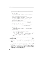
2674 Video Display Controller Write Cycle
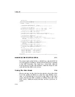
GROUPS [40-30,1][29-22][21-14][13][12][11][10][9][8][7][6][5-2]
DISPLAY HEX,HEX,HEX,BIN
! ADDR DATA CTRL UNUSED
! All - Al D15-D8 D7-D0 R U L P P R V V
! (A0) / D D S S E W D
! W S S 7 6 S A T
! - - - - - E I A
! T T C
! - - K
! -
! WRITE CYCLE addr $f0013, data $XX00 (addr $fxxxx = PS7-, data $XX00 =
LDS-)
1 $013 $XX $XX 1 1 1 1 1 1 X X XXXX
2 $013 $XX $00 0 1 0 0 1 1 X X XXXX
WAIT -
3 $013 $XX $00 1 1 1 1 1 1 X X XXXX
STOP
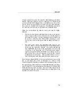
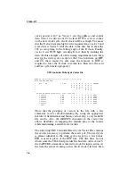
Eleven address lines go to the video board for addressing the
controller and video RAM. In a 68000-based system, A0
determines if the access is LDS or UDS. To provide a more
readable vector file, the unused pin 1 in the previous example is
assigned to be A0. (The LDS/UDS information is still contained
under the control section of the vector file.)
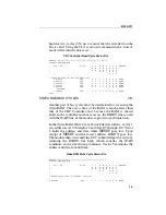
The first vector in this file sets the address. Vector 2, which is
driven 200 ns later, holds the address, sets the data, sets R/W and
LDS low (to get WR low), and sets PS7 low (to get CE low).
The WAIT statement ensures that VDTACK is returned before
continuing, The final vector, which is driven 200 ns later, holds
the address and data while the CTRL signals are changed to
return WR and CE high, thereby latching the data. Compare the
write cycle described above with Figure 7-2 to confirm that the
requirements for writing to the SCN 2674 are met.
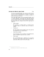
Determining the Read Cycle
7.16.
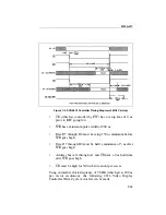
Examine the SCN2674 4 MHz read cycle timing diagram
(Figure 7-2) to learn how its signals interface with the video
board. To perform a read cycle, the following events must occur:
•
Address bus All through A1 must be set a minimum of 30
ns prior to RD going low (R/W high and LDS low).
Summary of Contents for 9100A Series
Page 6: ...vi ...
Page 8: ...viii ...
Page 10: ...x ...
Page 14: ...9100A 017 1 4 ...
Page 24: ...9100A 017 3 6 ...
Page 44: ...9100A 017 5 4 ...
Page 58: ...9100A 017 6 14 ...
Page 83: ...A 1 Appendix A New TL 1 Commands ...
Page 84: ...9100A 017 A 2 ...
Page 87: ...clockfreq 3 For More Information The Overview Of TL 1 section of the Programmer s Manual ...
Page 88: ...clockfreq 4 ...
Page 91: ...drivepoll 3 For More Information The Overview Of TL 1 section of the Programmer s Manual ...
Page 92: ...drivepoll 4 ...
Page 104: ...vectordrive 4 ...
Page 107: ...vectorload 3 For More Information The Overview Of TL 1 section of the Programmer s Manual ...
Page 108: ...vectorload 4 ...
Page 116: ...9100A 017 C 2 ...
Page 117: ...9100A 017 C 3 ...
Page 118: ...9100A 017 C 4 ...

