Options
Prescaler
This extra HF input (PM9624) is easily recognized by its front panel
connector (Input C, type N).
–
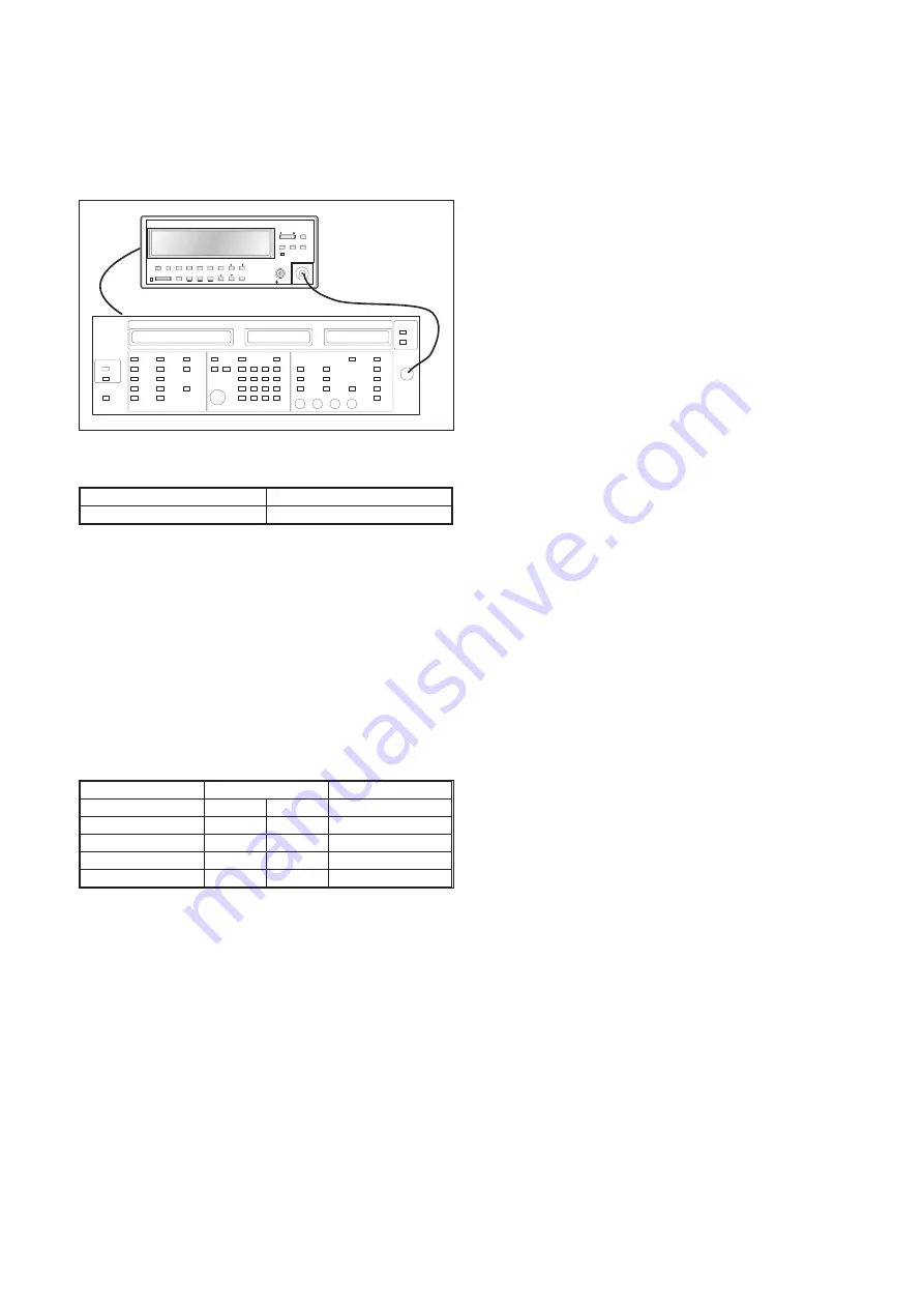
Connect the output of the signal generator to the HF input of
the counter.
–
Connect the 10 MHz REFERENCE OUT of the generator to
the REFERENCE IN at the rear panel of the counter.
Setting for the
counter
after Preset.
–
Function = FREQ C.
–
EXT REF.
Generate a sine wave in accordance with the following table.
–
Verify that the counter counts correctly. (The last digit will be
unstable).
Performance Check, Options 2-5
Frequency
Amplitude
Pass/Fail
MHz
mV
RMS
dBm
100-300
20
–21
-2500
10
–27
-2700
20
–21
-3000
100
–7
Table 2-7
Sensitivity of the PM9624 HF input.
EX T
RE F
Fig 2-2
Connect the output of the signal generator to the HF
input of the counter.
Required Test Equipment
Suggested Specification
HF signal generator
3.3 GHz
Table 2-8
Test equipment for 3.0 GHz HF input.
Summary of Contents for PM6685
Page 1: ...Programmable Frequency Counter PM6685 PM6685R Service Manual ...
Page 4: ...This page is intentionally left blank ...
Page 5: ...Chapter 1 Safety Instructions ...
Page 7: ...Chapter 2 Performance Check ...
Page 12: ...This page is intentionally left blank 2 6 Performance Check Options ...
Page 13: ...Chapter 3 Disassembly ...
Page 16: ...This page is intentionally left blank 3 4 Disassembly PM9691 or PM9692 Oven Oscillator ...
Page 17: ...Chapter 4 Circuit Descriptions ...
Page 33: ...Chapter 5 Repair ...
Page 42: ...This page is intentionally left blank 5 10 Safety Inspection and Test After Repair ...
Page 43: ...Chapter 6 Calibration Adjustments ...
Page 49: ...Chapter 7 Replacement Parts ...
Page 53: ...Replacement Parts Mechanical Parts 7 5 80 Lug bent 15 to lock ...
Page 62: ...This page is intentionally left blank 7 14 Replacement Parts GPIB Interface PM9626B ...
Page 63: ...Chapter 8 Drawings Diagrams ...
Page 65: ...This page is intentionally left blank Drawings Diagrams 8 3 ...
Page 66: ...Main PCB Component layout 8 4 Drawings Diagrams Top View ...
Page 68: ...Main PCB Component layout 8 6 Drawings Diagrams Bottom View K2 K1 K3 K4 ...
Page 70: ...This page is intentionally left blank 8 8 Drawings Diagrams ...
Page 72: ...8 10 Drawings Diagrams This page is intentionally left blank ...
Page 74: ...8 12 Drawings Diagrams This page is intentionally left blank ...
Page 76: ...Display Keyboard PCB Component layout 8 14 Drawings Diagrams ...
Page 78: ...GPIB Unit PM9626B Component layout 8 16 Drawings Diagrams ...
Page 79: ...GPIB Unit PM9626B Drawings Diagrams 8 17 ...
Page 80: ...This page is intentionally left blank 8 18 Drawings Diagrams ...
Page 81: ...Chapter 9 Appendix ...
Page 89: ...Replacement Parts 9 9 This page is intentionally left blank ...
Page 90: ...Power Supply Component layout 9 10 Replacement Parts BOTTOM SIDE TOP SIDE ...


