background image

Oscillator

n

Standard Oscillator

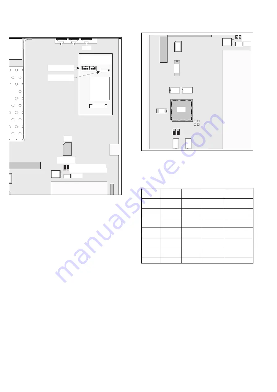
Be sure the jumpers J23 and J25 are in the STD position, (see

Fig. 5-4).

Check that 10 MHz is present at U29, pin 42.

Check that 10 MHz is present at the rear panel connector

10 MHz OUT (J27).

If you find any fault, continue with traditional troubleshooting tech-

niques and replace defective circuits. Also refer to Chapter 4, Circuit

Descriptions, Oscillator Circuits.

n

OCXO, PM9691 or PM9692

This test can be carried out only if the counter is equipped with one of

the optional oscillators, PM9691 or PM9692.

Be sure the jumpers J23 and J25 are in the OPT position, (see

Fig. 5-4).

Check that 10 MHz is present at U29, pin 42.

Check that 10 MHz is present at the rear panel connector

10 MHz OUT (J27).

These oscillators cannot be repaired in a local workshop. They must

be sent to the factory for repair.

Microcontroller

Check that 6 MHz is present at U11, pin 65 (see Fig.5-3).

Check that the RESET circuit U10 works properly by moving

the RESET jumper J29 temporarily to the ON position.

If the CPU is not running, check the state of the pins J11-J13. See ta-

ble below.

If you find any fault, continue with traditional troubleshooting tech-

niques and replace defective circuits. Also refer to Chapter 4, Circuit

Descriptions.

NOTE: Check that activity is going on at U11 pin 62 (ALE), pin

61 (RD), pin 63 (INST), and pin 43 (READY). These

pins should not be stuck HIGH or LOW.

If one or more bits on the AD-bus are corrupt, the

microcontroller (

m

C) often reads the same instructions re-

peatedly. When the

m

C discovers an invalid OP code, it will

RESET itself and start from the beginning again. The

m

C

sets the RESET input low when it resets itself. This can be

discovered at the RESET input of U11, (pin 16). If +5 V to

U10 is OK, this could be the cause of trouble.

5-6 Troubleshooting

U11

J1

1

J1

2

J1

3

J1

4

J29

J30

10

27

44

1

61

Stand

C11

B2

Optio

14

1

B1

U23

U17

U16

U2

2

U1

3

U1

4

Fig. 5-3

Test points and jumpers for checking the

microcontroller.

r

e

U29

Standard oscillator

C115

B2

J24

Optional OCXO

Optional oscillator

J23 J25

31

81

1

51

1

U23

Coarse adjust

Fine adjust

J27

Fig 5-4

Trimmers for the reference frequency oscillators.

Display

JP11, J12,

J13

Message

Error

Action

0.1

0, 0, 1

-

m

C I/O port

error

Replace U11

0.1.2

0, 1, 0

Err UC

m

C internal

RAM error

Replace U11

0.1.2.3

0, 1, 1

Err UC

m

C timer er-

ror

Replace U11

0.1.2.3.4

1, 0, 0

Err rA

RAM error

Replace U22

0.1.2.3.4.5

1, 0, 1

Err ASIC

ASIC error

Replace U29

All seg-

ments

1, 1, 0

1, 1, 1

Err rA

GPIB RAM

error

Replace U111 on

GPIB board

Test OK

Table 5-8

Start-up test.

Summary of Contents for PM6685

Page 1: ...Programmable Frequency Counter PM6685 PM6685R Service Manual ...

Page 2: ...ed in Sweden This is a complementary service manual covering instruments with manufacturing numbers exceeding 840684 The principal differences are to be found in Chapter 7 and in Chapter 8 due to a major redesign of the main PCB Do not dispose of the previous edition identified by the part number 4822 872 25012 and the publishing date June 1996 You may have to refer to it for information on older ...

Page 3: ...tenance 5 2 Calibration 5 2 When to Replace the Fan PM6685R only 5 3 Troubleshooting 5 4 General 5 4 Safety Inspection and Test After Repair 5 9 General Directives 5 9 6 Calibration Adjustments Introduction 6 2 Preparation 6 2 Power Supply 6 2 Input Amplifier 6 3 Reference Oscillators 6 4 Other Options 6 6 7 Replacement Parts Introduction 7 2 Mechanical Parts 7 3 Main Board 7 6 Front Board 7 12 GP...

Page 4: ...This page is intentionally left blank ...

Page 5: ...Chapter 1 Safety Instructions ...

Page 6: ...ocket outlets with protective ground contacts No other method of grounding is permitted for this instrument The ground symbol on the rear panel indicates where the protective ground lead is connected inside the instrument Never remove or loosen this screw When the instrument is brought from a cold to a warm environment condensation may cause hazardous conditions Therefore ensure that the grounding...

Page 7: ...Chapter 2 Performance Check ...

Page 8: ... Microprocessor RAM ROM Measuring circuits Display If a GPIB interface is installed the GPIB address is displayed If there are any test failures an error message is shown Turn on the counter and check that all segments light up on the display and that no error message appears Internal Self Tests The different built in test routines invoked by the power on test can also be activated from the front ...

Page 9: ...cordingly See the Pre ventive Maintenance in the Repair chapter Chapter 5 To check the accuracy of the oscillator you must have a calibrated reference signal that is at least five times as stable as the oscillator that you are testing see the following table Press the PRESET key then press the ENTER key to set your counter in the Default setting Performance Check Short Form Specification Test 2 3 ...

Page 10: ... Hz 5 LSD EXT ARM INPUT Press the PRESET key then press the ENTER key to set your counter in the Default setting Select 50 W input impedance Apply 10 MHz 500 mVRMS 1 4 VPP sine to input A The counter measures and displays 10 MHz Press the AUX MENU key Press the DATA ENTRY UP DOWN keys until the display shows Ar Start confirm by pressing the ENTER key Press DATA ENTRY UP DOWN keys until the display...

Page 11: ...ion FREQ C EXT REF Generate a sine wave in accordance with the following table Verify that the counter counts correctly The last digit will be unstable Performance Check Options 2 5 Frequency Amplitude Pass Fail MHz mVRMS dBm 100 300 20 21 2500 10 27 2700 20 21 3000 100 7 Table 2 7 Sensitivity of the PM9624 HF input EX T RE F Fig 2 2 Connect the output of the signal generator to the HF input of th...

Page 12: ...This page is intentionally left blank 2 6 Performance Check Options ...

Page 13: ...Chapter 3 Disassembly ...

Page 14: ...se extreme caution WARNING Capacitors inside the instrument can hold their charge even if the instrument has been sepa rated from all voltage sources Make sure the power cord is disconnected from the counter Turn the counter upside down Loosen the two screws A at the bottom and the two screws B in the rear feet Grip the front panel and gently push at the rear Pull the counter out of the cover Rein...

Page 15: ...scillator Disconnect the power cable Remove the cover of the counter Remove the two screws A holding the oscillator to the main pca from underneath Press the clip B gently to the front of the counter and lift the oscillator straight up Make sure that jumpers J14 and J15 are set in the correct posi tion When fitting the oscillator make sure that the connector pins fit exactly in the holes in the co...

Page 16: ...This page is intentionally left blank 3 4 Disassembly PM9691 or PM9692 Oven Oscillator ...

Page 17: ...Chapter 4 Circuit Descriptions ...

Page 18: ...e front unit contains all functions needed for the user communica tion It is connected to the main board unit with a flat cable and the molded front unit is fixed to the two profiled aluminum rods with screws The main board unit consists of a PCB mounted on two profiled alu minum rods Most functions such as the following are placed on the main board Input amplifiers with trigger level circuits Pow...

Page 19: ... HF input Input Amplifier Reset circuit Power supply 90 265 V Micro computer Counter ASIC 10 MHz out Gate LED Display Analog output GPIB option Keyboard 7V 5V 5 2V AC I C 2 PWM E C D A G RESET U11 HSI 0 X2 EXTC B2 EXTREF A A2 U29 GET Trigger DAC s INTREF 2 12V Option 80 Fig 4 1 PM6685 block diagram ...

Page 20: ...t by the resistors R204 R207 The backlight dissipates approximately 1 5 W Keyboard The front panel pushbuttons are connected in a matrix The scanning signals H0 to H3 come from the main board If a push button is pressed and H0 to H3 is high one of the output signals V0 to V7 will be high The STAND BY ON and LOCAL PRESET buttons are not part of the scanning but are connected directly to the main bo...

Page 21: ... serves both as current limiter together with the voltage limiter see below and as impedance matching resistor The resistor also improves the Volt age Standing Wave Ratio VSWR of the amplifier input x1 x11 Attenuator The x1 attenuator consists of a resistive low frequency divider which reduces the input signal by a factor of 2 and a capacitive high frequency divider The attenuator is formed by the...

Page 22: ...ely 5 kHz The high frequency signal is fed to the gate of Q1 The high imped ance at the gate is converted to a low impedance at the source The source is connected to the base of HF transistor Q2 the summing point for the two signal paths To make the FET work well in its active region within the whole dy namic range the FET drain is supplied with 7 V via resistor R42 The low frequency signal is div...

Page 23: ... level in the range of approximately æ1 6 V This covers a dynamic range of 6 4 V since the input signal is divided by a factor of 2 before it reaches the comparator The counter is provided with adjustable hysteresis i e it is control lable via the front panel or GPIB The circuitry for setting the hyster esis consists of the resistor network R91 to R96 supplied with 5 V and 5 2 V It is connected to...

Page 24: ...ltiplexers U3 to select one of the levels With this arrangement there is a total trigger level range of 1 6 V to 1 6 V A double DAC U4 Two current to voltage converters U6 These circuits convert the current at the IOUT pins of the DACs to a voltage This signal has a range of 0 V to approximately 1 6 V Two amplifiers U7 with an amplification of X2 to generate a signal with a range of 0 V to 3 2 V R...

Page 25: ... resistor is cold but decreases to a few ohms as it is warmed up by the steady state current The AC voltage is rectified in the bridge rectifier D9 and filtered in C64 C65 suppresses noise from D9 L6 and C82 C83 serve as a fil ter at the input of U39 All inputs and outputs of the power module have HF chokes The module is mounted with distance washers on the main board From the module there are thr...

Page 26: ...D BY LED that is fed by the uninterruptible 12 V 5 V also indirectly controls the fan in the PM6685R It is a 12 V DC fan that operates only if 12 V is on An NTC resistor serving as a temperature sensor controls the speed by applying a variable refer ence voltage to the fan voltage regulator U42 Counter ASIC The main part of the counting logic is integrated in a CMOS ASIC specially designed for the...

Page 27: ...anel and selected by means of the EXT REF button on the front panel In addition to the standard crystal oscillator there are two optional oven controlled crystal oscillators OCXO to choose from Standard The uncompensated standard oscillator consists of the crystal B2 C109 C113 C115 R209 and R211 C115 is used for manual adjust ment of the frequency when the calibration tolerance has been ex ceeded ...

Page 28: ...lse is set by C88 2 2 µF gives a pulse of ap proximately 30 ms U10 also controls the reset pulse during power up so that the microcontroller will be initiated correctly n Keyboard Scanning The keyboard scanning is done in two modes The first mode is ac tive as long as no button has been detected as depressed Then all out puts of U13A are set high and the latch U14A is read If no button has been de...

Page 29: ...ar panel and connected to the main board with a flat cable Besides the normal standard GPIB connector this optional unit also has a BNC connector capable of outputting an analog representation of any three consecutive digits on the display There is also a 6 SPST DIP switch on this unit for setting the default GPIB address Hardware Functional Description 4 13 OF F ON G D E 16 8 4 2 1 R L1 D C1 DT 1...

Page 30: ...gnal is filtered attenuated offset adjusted inte grated and buffered by IC103 and supporting passive components to give an analog DC level between 0 and 4 98 V with a resolution of 20 mV The analog output has a separate analog ground connected to the cabinet HF Input You can add an optional prescaler This HF input is mounted on the main board to the right of the input amplifier It is connected to ...

Page 31: ...t output via the front panel except displaying the measurement results The PresetDevice procedure reprograms the complete device when the PRESET key has been pressed in local mode It aborts pending measurements TheExecuteGpibCommands procedure executes GPIB commands and if a query is received it starts the response formatter and sends the requested data to the GPIB interface If the display is swit...

Page 32: ...performed Write 001 to internal test pins Pulse all microcomputer i o ports twice Write 0 1 on display Write 0 1 2 on display and 010 on test pins Test mC internal RAM error Err mC halt Write 0 1 2 3 to display and 011 on test pins Test mC timer error Err mC halt Write 0 1 2 3 4 on display and 100 on test pins Test main board RAM error Err ra halt Write 0 1 2 3 4 5 to display and 101 to test pins ...

Page 33: ...Chapter 5 Repair ...

Page 34: ...rature of 20 to 30 C the temperature stability of an OCXO will be in creased by a factor of 3 The temperature stability indicated for the standard oscillator is mainly dependent on the ambient temperature When the coun ter is operating there is always an internal temperature increase that will influence the oscillator n Recalibration intervals The Mean Time Between ReCalibration MTBRC is defined a...

Page 35: ...ble on page 5 2 The results will be the following Relative Frequency deviation caused by Ambient temperature deviation within 0 to 50 C reference point at 23 C Less than 3 10 8 Aging year Less than 1 5 10 7 Use the MTBRC formula with the above values This gives a MTBRC of maximum 3 10 3 10 15 10 18 7 8 7 year NOTE When recalibrating the reference crystal oscillator will be compensated only for fre...

Page 36: ... in the PM6685 one on the main PCB containing the instrument firmware the other on the optional GPIB board containing the interface bus firmware They have labels with version designation of the traditional form Vx yz where x y and z are digits The last digit can be followed by a single letter The version numbers do not have to coincide except for the last letter So the combination Vr stE and Vu vw...

Page 37: ... input AC voltage If not use traditional troubleshooting tech niques to locate the fault Remove the power cable from the counter Measure the resistances according to the table below If one of the above mentioned measurements shows 0 W remove L7 L8 and L9 and use conventional troubleshoot ing techniques to isolate the fault Measure the resistances according to the table below If the resistances dev...

Page 38: ...ues and replace defective circuits Also refer to Chapter 4 Circuit Descriptions NOTE Check that activity is going on at U11 pin 62 ALE pin 61 RD pin 63 INST and pin 43 READY These pins should not be stuck HIGH or LOW If one or more bits on the AD bus are corrupt the microcontroller mC often reads the same instructions re peatedly When the mC discovers an invalid OP code it will RESET itself and st...

Page 39: ...pp to Input A Measure the AC levels according to Fig 5 5 Use the oscillo scope and a 10 MW probe If you find any fault continue with traditional troubleshooting tech niques and replace defective circuits Also refer to Input Amplifiers A and B in Chapter 4 Circuit Descriptions Troubleshooting 5 7 TP27 1 4V U8 Q1 Q3 Q4 U1 U9 Q13 0V 0 3Vpp 1 5V 0 6Vpp 0 6Vpp 0 8V 7V 0V 0 6Vpp 1Vpp 4 3V 0 8V 0 4V 3V 2...

Page 40: ...tion of the procedure to follow Large deviations indicate a fault Trace the signal through the inte gration chain with traditional troubleshooting techniques and replace defective circuits The duty cycle at U101 1 should be 50 Also re fer to GPIB Interface Including Analog Output in Chapter 4 Circuit Descriptions n Bus Interface A simple method to check the most fundamental functions of the in ter...

Page 41: ... the primary circuits are important to the safety of the instrument and may be replaced only by components obtained from your local Fluke representative Checking the Protective Ground Connection Visually Check the correct connection and condition and measure the resistance between the protective lead at the plug and the cabinet The resistance must not be more than 0 5 W During measurement the powe...

Page 42: ...This page is intentionally left blank 5 10 Safety Inspection and Test After Repair ...

Page 43: ...Chapter 6 Calibration Adjustments ...

Page 44: ...nect the DMM to test point TP15 5V and GND see Fig 6 2 Adjust the 5V trim potentiometer inside the power module until the DMM reads 5 10 0 01 V Check that the voltage between the test point TP23 5 V and GND is 5 06 0 03 V Check that the unregulated voltage from the power module at test point TP16 15 V is about 18 V Check that the unregulated voltage from the power module at test point TP17 7 V is ...

Page 45: ...has been correctly adjusted so that incorrect observations of undershoots overshoots are not made Use the probe to connect channel B of the oscilloscope to Pin 10 of U8 Adjust R31 LIN A until both signals look as alike as possi ble NOTE The AC coupling will give the curve a slight tilt x1 Attenuator n Setup Adjust C2 X1 until both signals on the screen look as alike as possible without any oversho...

Page 46: ...er reads 100 Hz NOTE Reinstall the screen shield after making these adjust ments Reference Oscillators NOTE The standard oscillator is always mounted in the unit even if an optional oscillator is installed You set the jumpers J23 and J25 to select the timebase source that you want to use Standard Oscillator n Setup Connect the counter to line power Switch on the counter Press PRESET then press ENT...

Page 47: ...o compen sate for the aging that occurs during at least two years of operation Fine adjustment Adjust the trimmer to better than 10 MHz 0 2 Hz PM9691 or 10 MHz 0 05 Hz PM9692 i e 20 resp 5 in the last two digits on the PM6681R PM6685R display If this adjustment is OK reassemble the counter Coarse adjustment Make this adjustment only if the trimmer range is insufficient to ad just the oscillator Re...

Page 48: ...keys until the display reads ANALOG OUT Press ENTER Press DATA ENTRY UP DOWN keys to select ON Press ENTER Press DATA ENTRY UP DOWN keys to until the display reads 1 0 3 V Press ENTER Connect the LF synthesizer to the A input of the counter The counter should read 1000 0xxxxx Hz n Adjustment Adjust the trimmer ZERO see Fig 6 6 until the output volt age is 0 V 1 mV Set the LF synthesizer to 999 90 ...

Page 49: ...Chapter 7 Replacement Parts ...

Page 50: ...ronic components the following special components are used Components that are manufactured or selected by the manufac turer to meet specific performance requirements Components that are important for the safety of the instrument Both types of components may be replaced only by components ob tained through your local Fluke organization NOTE Physical size and shape of a component may af fect the pe...

Page 51: ...4 R 58 Tilting support 5322 401 11471 R 62 Coax connector 5322 267 10004 S 63 Coax connector 5322 265 10264 R 64 Soldering tag 9 6X15 15 ms fs 5322 290 30318 S 67 Toroid core 30nh rcc9 6 3 4c65 violet 5322 526 10545 P 68 Bottom shield 5322 447 91829 P 70 BNC holder 4031 100 48830 P 84 Mains filter 1a fs3514 1 07 5322 121 42352 R 90 PCA guide for prescaler 5322 401 11347 P 92 Stand off nut M3x14 40...

Page 52: ...Screw rtk ko st3 5X10 stfz 5322 502 30703 P 180 Spring washer kba 3 2 St fz din137 4822 530 80173 P Pos Description Part Number P 182 Spring washer kba 4 3 St fz din137 4822 530 80076 P 184 Lock washer yt4 3 St fz din6798a 4822 530 80083 P 190 Nut m6m 04 st fzb 4822 505 10326 P 200 Receptacle 140825 2 2 8X0 8 5322 268 10275 P 201 Protect sleeve 2 8mm N 94610 transp pa 5322 321 40117 P 202 Cable cl...

Page 53: ...Replacement Parts Mechanical Parts 7 5 80 Lug bent 15 to lock ...

Page 54: ...NP0 0805 5322 126 14051 S C154 CAPACITOR 22 pF 5 50V NP0 0805 5322 122 32658 S Pos Description Part No P C155 CAPACITOR 10 nF 20 50V X7R 0805 5322 122 34098 S C156 CAPACITOR 15 UF 20 6 3V 6 0X3 2 MOLD 5322 124 11418 S C157 CAPACITOR 15 UF 20 6 3V 6 0X3 2 MOLD 5322 124 11418 S C158 CAPACITOR 100 nF 20 25V X7R 0805 5322 126 13638 S C159 CAPACITOR 100 nF 20 25V X7R 0805 5322 126 13638 S C16 CAPACITOR...

Page 55: ...R 10 nF 20 50V X7R 0805 5322 122 34098 S C98 CAPACITOR 10 nF 20 50V X7R 0805 5322 122 34098 S C99 CAPACITOR 10 nF 20 50V X7R 0805 5322 122 34098 S D1 DIODE 0 10A BAT18 35V 1PF SOT23 5322 130 32076 S D10 DIODE 1A SB140 40V DO41 5322 130 81917 S Pos Description Part No P D12 DIODE 0 10A BAV99 SOT23 5322 130 34337 S D13 DIODE 0 10A BAV99 SOT23 5322 130 34337 S D14 DIODE 0 10A BAV99 SOT23 5322 130 343...

Page 56: ...1W 100PPM 0805 5322 117 12497 S R109 RESISTOR 100 ohm 1 0 1W 100PPM 0805 5322 117 12497 S R11 RESISTOR 120 ohm 1 0 125W 100PPM 1206 4822 051 10121 S R110 RESISTOR 100 ohm 1 0 1W 100PPM 0805 5322 117 12497 S R111 RESISTOR 100 ohm 1 0 1W 100PPM 0805 5322 117 12497 S R112 RESISTOR 100 ohm 1 0 1W 100PPM 0805 5322 117 12497 S R113 RESISTOR 100 ohm 1 0 1W 100PPM 0805 5322 117 12497 S R115 RESISTOR 10 0 ...

Page 57: ...100PPM 1206 5322 117 10034 S R244 RESISTOR 82 ohm 1 125W 100PPM 1206 4822 051 10829 S Pos Description Part No P R245 RESISTOR 3 90 kohm 1 125W 100PPM 1206 4822 051 53902 S R247 RESISTOR 820 ohm 1 125W 100PPM 1206 5322 116 82264 S R248 RESISTOR 680 ohm 1 125W 100PPM 1206 4822 051 56801 S R249 RESISTOR 47 ohm 1 0 1W 100PPM 0805 5322 117 12505 S R25 RESISTOR 470 kohm 1 125W 100PPM 1206 5322 116 80447...

Page 58: ... 051 51003 S R66 RESISTOR 4 70 kohm 1 125W 100PPM 1206 4822 051 54702 S R67 RESISTOR 2 20 kohm 1 125W 100PPM 1206 4822 051 52202 S R69 POTENTIOMETER 100 kohm 3304X 1 104 5322 101 10841 S R7 RESISTOR 120 ohm 1 0 125W 100PPM 1206 4822 051 10121 S R70 POTENTIOMETER 100 kohm 3304X 1 104 5322 101 10841 S Pos Description Part No P R71 RESISTOR 100 kohm 1 0 125W 100PPM 1206 4822 051 51004 S R72 RESISTOR ...

Page 59: ... 61813 S U43 CLAMP TO220 5322 401 11257 P U43 IC 1 50 A LM337T TO 220 5322 209 81236 S U44 IC CMOS 74HC125 SMD SO14 9337 569 90701 S U5 IC NE532D DUAL SO 8 5322 209 71553 S U50 IC COMP MAX961 SO8 4 5ns 9322 194 34682 R U6 IC NE532D DUAL SO 8 5322 209 71553 S U7 IC NE532D DUAL SO 8 5322 209 71553 S U8 IC COMP AD96687BP PLCC20 4822 201 62795 R U9 IC DIG ECLIPS MC10E104 4822 209 31775 R Replacement P...

Page 60: ...or 10 nF 20 50V X7R 0805 5322 122 34098 S D201 LED 3 mm HLMP 1300 red 5322 130 81921 R Pos Description Part Number P D202 LED 3mm Yellow 590nm 4 8MCD 10mA 4822 130 30953 R P204 Connector 40 POL TMH 120 01 L DW 5322 265 51295 P R201 Resistor 220 k 1 125W 100PPM 1206 4822 051 52204 S R204 Resistor 10 0 W 1 0 125W 1206 4822 051 10109 S R205 Resistor 10 0 W 1 0 125W 1206 4822 051 10109 S R206 Resistor...

Page 61: ... 63475 S IC103 IC NE532D DUAL SO 8 5322 209 71553 R IC106 IC PC74HC00T SO14 5322 209 71802 S IC107 IC PC74HC573T SO20 5322 209 60424 S IC108 IC PC74HC573T SO20 5322 209 60424 S IC109 IC socket 32pin P N 213 032 602 5322 255 41141 S IC109 IC PROM PM9626B 5322 209 51853 R IC111 IC SRAM TC55257DFL 85L SOP28 32Kx8 9322 106 65682 R IC113 IC DIG UPD7210D IEC BUS GPIB CONTROLLER 9322 023 60682 R IC114 IC...

Page 62: ...This page is intentionally left blank 7 14 Replacement Parts GPIB Interface PM9626B ...

Page 63: ...Chapter 8 Drawings Diagrams ...

Page 64: ... designed to be logical and easy to read The component number is written above the symbol Inside the symbol at the top is an abbreviated description of the cir cuit s function Pin numbers are written outside the symbol and if it is a complex cir cuit the pin functions are written inside A small circle on a pin indicates that the input output inverts the sig nal The component name is written below ...

Page 65: ...This page is intentionally left blank Drawings Diagrams 8 3 ...

Page 66: ...Main PCB Component layout 8 4 Drawings Diagrams Top View ...

Page 67: ...8 RDX P2 1 17 EXTINT P2 2 15 T2CLK P2 3 44 T2RST P2 4 42 PWM P2 5 39 P2 6 33 P2 7 38 CLKOUT 65 WR WRL 40 BHE WRH 41 RD 61 ALE ADV 62 INST 63 AD0 P3 0 60 AD1 P3 1 59 AD2 P3 2 58 AD3 P3 3 57 AD4 P3 4 56 AD5 P3 5 55 AD6 P3 6 54 AD7 P3 7 53 AD8 P4 0 52 AD9 P4 1 51 AD10 P4 2 50 AD11 P4 3 49 AD13 P4 5 47 AD14 P4 6 46 AD15 P4 7 45 AD12 P4 4 48 HSI 0 24 HSI 1 25 HSO 4 HSI 2 26 HSO 5 HSI 3 27 HSO 0 28 HSO ...

Page 68: ...Main PCB Component layout 8 6 Drawings Diagrams Bottom View K2 K1 K3 K4 ...

Page 69: ... 56 R321 10 Q27 BFG16A C102 33pF L15 BLM21A102S C134 10n R314 120 BNC Coax R217 100 R258 100 C136 15uF 6 3V TP28 R250 Not used R296 220 C127 1n C178 100nF L11 BLM21A102S R317 220 R241 10K C123 47p C130 100nF R220 1K B2 10MHz R330 47 R309 47 R316 2 2K BAV99 D19 R320 56 Q35 BFS17 L14 BLM21A102S R52 Not used J27 BNC Coax R218 680 1 U25D HC32 12 13 11 R219 330K Q32 BFS17 C113 82p R243 18K C132 2 2uF 6...

Page 70: ...This page is intentionally left blank 8 8 Drawings Diagrams ...

Page 71: ...C27 10n R119 1K R46 150 D2 BAT18 R66 4 7K R69 100K C29 100nF R81 10K C24 10n K4A 3 4 2 C39 6 8u 16V R63 6 8K TP11 C56 10n C54 10n R34 18K R15 150 TP27 C45 100nF R44 47 R58 120 R77 10K C55 100nF C5 10n L1 220uH Q2 BFR92A R89 68 R20 8 2K U1A 3140 2 3 6 1 8 5 R73 10K R10 120 R113 100 R21 15 R39 R100 10M R40 47 27 R28 470K L23 4S2 3 5X6MM U7A NE532D 2 3 1 U9B 10E104 2 3 10 9 U4 PM7258 CS 15 WR 16 DACA...

Page 72: ...8 10 Drawings Diagrams This page is intentionally left blank ...

Page 73: ...0K R144 220 R56 390 R149 220 BAV99 D13 TP15 5V R156 2 2K R140 220 C71 10n C104 10n R206 5 6K Q14 BC847B R136 220 R196 120 R53 2 2K K5B 13 9 11 R129 470 1 25V U _ _ U42 LM317T 3 2 1 R132 220 U40C HEF4013BT VCC 14 GND 7 J15 TP16 15V S 1D C1 R U40A HEF4013BT 6 5 3 4 2 1 F1 1 6AT L6 10mH R154 220 9 99 U39 POWER MODULE 6 7 8 9 10 11 13 14 PF 12 DCIN 1 DCIN 4 DCIN 5 C64 270uF J3 Q7 BC807 25 1 25V REG U4...

Page 74: ...8 12 Drawings Diagrams This page is intentionally left blank ...

Page 75: ...2 S H 3 RD 4 CS 5 VREF 7 VIN 8 VREF 9 DB2 18 DB1 19 DB0 20 DB6 14 DB5 15 DB4 16 DB3 17 DB7 13 DB8 12 DB9 11 L20 BLM21A102S C174 100nF R285 33K C164 2 2uF 6 3V U34B HC00 4 5 6 C156 15uF 6 3V R294 C149 22p C169 10n 10n U44C HC125 9 8 10 U35A ADC1061 INT 2 S H 3 RD 4 CS 5 VREF 7 VIN 8 VREF 9 DB2 18 DB1 19 DB0 20 DB6 14 DB5 15 DB4 16 DB3 17 DB7 13 DB8 12 DB9 11 U38C NE532D V 8 V 4 U34D HC00 12 13 11 R...

Page 76: ...Display Keyboard PCB Component layout 8 14 Drawings Diagrams ...

Page 77: ...04 P204 P204 P204 EXT REF S201 CHECK S202 MEAS RESTART S209 DISP HOLD S210 FUNCTION S216 STAND BY IND GATE IND SCL SDA ON ON S222 R204 10 R205 10 R206 10 D201 D202 CQV13 6 YELLOW RED HLMP K150 R207 10 LOCAL PRESET BACK LIGHT TEMP COMP 5V GND NC 5V 5V 11 7 8 9 5 10 5 11 7 8 9 10 5V 5V 5V 5V 5V C202 10n C201 10n IC TYPE BACKLIGHT D203 DL100 U201 PCF8576 PCF8576 PCF8576 PCF8576 U202 GND SYNC SYNC DIS...

Page 78: ...GPIB Unit PM9626B Component layout 8 16 Drawings Diagrams ...

Page 79: ...GPIB Unit PM9626B Drawings Diagrams 8 17 ...

Page 80: ...This page is intentionally left blank 8 18 Drawings Diagrams ...

Page 81: ...Chapter 9 Appendix ...

Page 82: ...w 9 2 How to Replace Surface Mounted Devices Fig 9 1 Heat the leads and push a thin aluminum sheet between the leads and the PC board Fig 9 2 When removed clean the pads with desoldering braid Fig 9 3 Place solder on the pad Fig 9 4 Attach the IC to the pad with the solder Fig 9 5 Solder all leads with plenty of solder don t worry about short circuits at this stage Fig 9 6 Remove excessive solder ...

Page 83: ...s how you can minimize the risk of damage or destroying these devices by being aware of the problems and learning how to handle these compo nents ESD sensitive options are packed in conductive containers marked with the symbol to the leftl Never open the container unless you are at an ESD protected work station Use a wrist strap grounded via a high resistance Use a grounded work mat on your work b...

Page 84: ...bus An internal address and data bus for communi cation between microcontroller measuring logic and options IEC 1010 1 International Electrical Commission safety standard L LSI Large Scale Integrated circuit O OCXO Oven Controlled X tal Oscillator P PCA Printed Circuit Assembly PCB Printed Circuit Board Performance Check A procedure to check that the instrument is functionally operational and perf...

Page 85: ...e voltage has reached the internal reference level in U03 the switch transistor V01 is turned off V05 is a blanking transistor that will compensate for high transients generated by the transformer T01 The internal sawtooth generator RC pin 7 in U03 is connected to the SENSE input via V03 to compensate for low load The regulated 5 V is sensed by U01 and adjusted by R50 The out put of U03 is connect...

Page 86: ...e between pin 1 and 4 on T01 is about Ö2 times the input AC voltage If not use traditional faultfinding techniques to locate the fault Disconnect the secondary load by moving the jumper J16 to its alternative position Check the STAND BY voltages according to Table 9 2 Restore the jumper J16 to its normal position Check the waveforms in Fig 9 10 at the corresponding testpoints in Fig 9 9 to verify ...

Page 87: ...reach normal oper ating temperature n Setup Connect the counter to the line power Switch on the counter Press PRESET then press ENTER n Adjustment CAUTION If you adjust the 5 V trimmer you have to adjust the complete instrument Connect the DMM between TP23 and ground see Fig 9 11 Adjust the 5 V trimmer potentiometer R50 in the power sup ply through the nearest vent in the protective cover until th...

Page 88: ...2 Resistor 10 0 kW 1 0 125W 4822 051 51003 R13 Resistor 10 0 kW 1 0 125W 4822 051 51003 R14 Resistor 10 0 W 1 0 125W 4822 051 51003 R15 Resistor 10 0 kW 1 0 125W 4822 051 51003 R16 Resistor 10 0 kW 1 0 125W 4822 051 51003 Pos Description Part Number P R17 Resistor 10 0 kW 1 0 125W 4822 051 51003 R18 Resistor 10 0 kW 1 0 125W 4822 051 51003 R19 Resistor 10 0 kW 1 0 125W 4822 051 51003 R20 Resistor ...

Page 89: ...Replacement Parts 9 9 This page is intentionally left blank ...

Page 90: ...Power Supply Component layout 9 10 Replacement Parts BOTTOM SIDE TOP SIDE ...

Page 91: ...00K R27 100K V01 BUK 446 R28 10K D08 B ZX84C18 D09 BA V23 D09 B AV23 R29 4 7 D11 BZ X84C18 C12 100U 35V R30 10K R31 100K R32 100K D12 BZX84C18 D13 BZ X84C8V 2 C13 220P R33 10 R34 1K R35 2 7 R36 2 7 R37 2 7 R38 1K C14 100P R39 10 V04 BC817 D14 BA V23 R40 100 R41 100 C15 22P D14 BAV23 R42 1K V05 BC817 R43 100 R44 100 C16 4 7N C17 4 7N R45 1K C18 100N C19 100N C20 100N R46 C21 470U 35V C22 470U 35V C...

Page 92: ...the Rubidium time base is still in its warm up phase and is not yet stabilized Test procedure Connect the counter to the line power Check that the UNLOCK LED is lit Check that the UNLOCK LED is switched off within 6 minutes after connection to line power Connect a 10 MHz reference signal to input A of the counter Select FREQUENCY A measurement Select 1 s measuring time Check that the displayed fre...

Page 93: ...efore Calibration Adjustment the Rubidium time base must have been in operation for more than 24 hours Required Test Equipment Setup Connect the counter to the line power Press PRESET then ENTER Press AUX Calibration Adjustments 9 13 Type Performance Model 10 MHz reference 1x10 10 Calibrated Rubidium oscillator or Cesium atomic standard Table 9 5 Required test equipment A2 RUBIDIUM OSCILLATOR TYPE...

Page 94: ...ith a relevant seal if necessary Replacement Parts Pos Description Part Number P Cover incl front part 5322 447 92194 P Fan 2822 031 01327 R Text plate kit 4031 100 62440 R Rear plate 4031 100 53930 P A1 Power supply 5322 214 91268 P D1 LED HLMP 1300 red 5322 130 81921 L1 Toroid 5322 526 10545 L2 Toroid 5322 526 10545 L3 Toroid 5322 526 10545 P1 P3 Cable kit 4031 100 61530 P R1 Potentiometer 1 kW ...

Reviews: