


M
ODEL
SDP100 V
ERSION
V_1.00
P
REPARED BY
H/W
D
ATE
25/05/2007
S
UBJECT
T
ECHNICAL
M
ANUAL
P
AGE
1/70
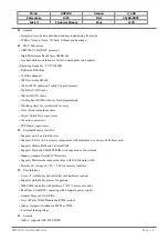
Baseband section
This document provides a description of the baseband section of the SDP100. Most design decisions are explained,
but no detailed calculations are included. Total chip solutions(MT6228, MT6305BN, MT6120) except for RF
Power Amplifier(RF3166) are from MediaTek, Taiwan.
I. MT6228 ( GSM/GPRS Baseband Processor )
1.
System OverView
The Revolutionary MT6228 is a leading edge single-Chip solution for GSM/GPRS mobile phones targeting the emerging
applications in digital audio and video. Based on 32bit ARM7EJ-S
TM
RISC processor, MT6228 not only features high
performance GPRS Class 12 MODEM, but also provides comprehensive and advanced solutions for handheld multi-
media. But, the SDP100 can only support GPRS Class 8.
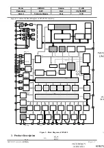
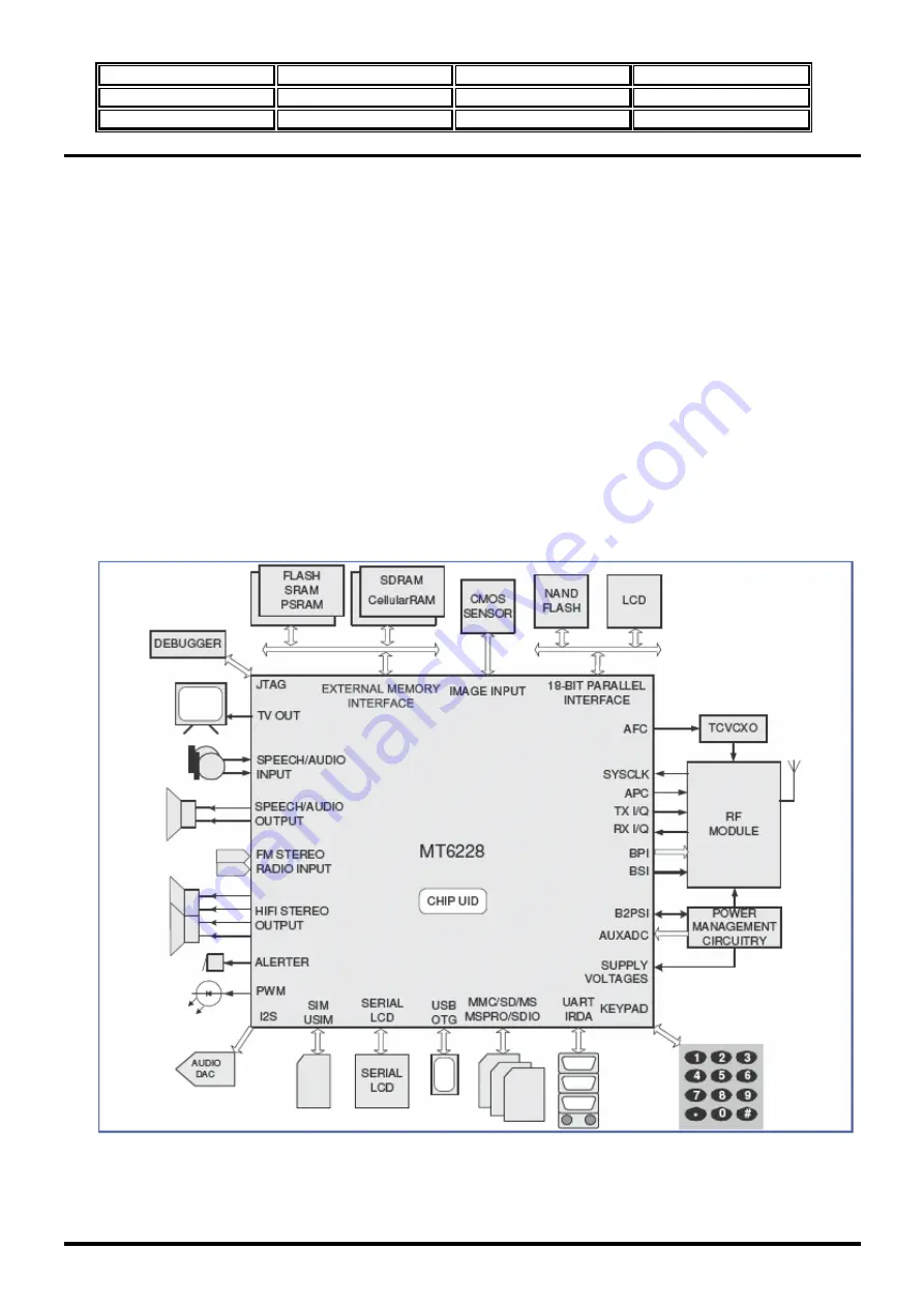
The Figure 1 is shown Typical Application for MT6228.
Figure 1 : Typical Application for MT6228
1.1
Platform Feature
SDP100
T
ECHNICAL
M
ANUAL
Page 3.1


