background image


Page 6 of  28 

Rev. A 


2.6 

CPU  ( MOTOROLA/ MC68HC908JL8CSP)  

The Central Process Unit 
 

2.7 

Electricity Sw itch 

I t controls the + 5Vdc and + 12Vdc supplies. 
+ 5Vdc and + 12Vdc Control Power Generator. 
P 5Vdc (generated from 7805 regulator) and + 12Vdc power supply. 
 

2.8 

Charger: 

The source for the Charger comes from the mains through the transformer and 
full-bridge inverter.  The charger is controlled with high frequency technology and 
the acceptable charging voltage is 13.6~ 13.9V. 
 

2.9 

I nverter Circuit: 

The inverter circuit is based on a full-bridge circuitry. 


2.10  I nterface Circuit: 

Vesta 1000: The UPS display device contains three LEDs and one switch. 
Vesta 1500/ 2000: The UPS display device contains six LEDs and one switch. 
 

2.11  Batteries: 

Acts as a power supply source while the UPS is on battery mode. Different types 
of batteries are used for different models of UPS: 
1000VA: 12V7Ah * 2 pcs or equal capability 
1500VA: 12V45W * 2 pcs or equal capability 
2000VA: 12V45W * 2 pcs or equal capability 


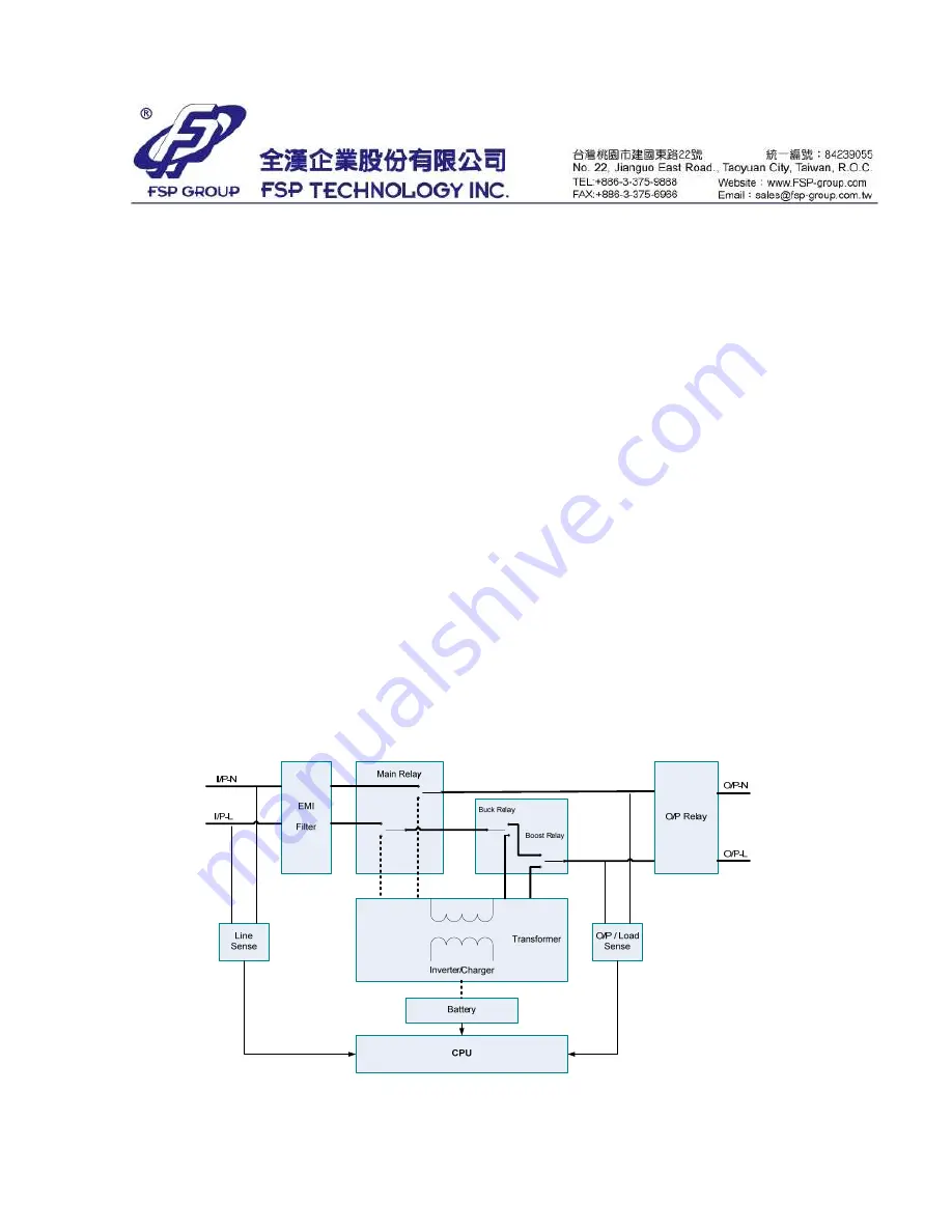
Figure S- 1     Block Diagram 

Summary of Contents for 1500 Series

Page 1: ...л чит т нич ю н льт цию гл т чн Б з вы дны www sotmarket ru д бн я инф м ция т в тзывы бз ы и ы Инструкция для FSP EP 1000 Перейти в карточку товара 8 800 775 98 98 ...

Page 2: ...Page 1 of 28 Rev A UNINTERRUPTIBLE POWER SYSTEM SPECIFICATION EP 1000 1500 2000 Series ...

Page 3: ...Page 2 of 28 Rev A 1 0 Revision Summary REVI SI ON SECTI ON DESCRI PTI ON Rev A Formal Release ...

Page 4: ...Circuit 7 4 Battery Charger 9 5 Line and Zero Crossing Detection 11 6 I nverter Operation 13 7 Active Clamp 16 8 Microprocessor CPU Control Circuit 17 9 Relay Circuit 19 10 Display Audio Alarm and Control Button 21 11 Load Detection Circuit 23 12 I nterface Circuit 24 13 Troubleshooting 25 ...

Page 5: ... point the AVR will be activated and decrease the input voltage by 0 85 times of incoming utility voltage Buck activated point 110 VAC 120 VAC 220 VAC 230 VAC 240 VAC 121 VAC 132VAC 242 VAC 253 VAC 264VAC 1 3 50 60Hz Automatic Frequency Selection The output frequency will automatically match the input frequency 50 or 60Hz 1 4 Communication Port USB It provides remote shutdown capability via commun...

Page 6: ...ck activated point Refer to Buck activated point table in P 4 Relay OFF line voltage is normal Relay ON line voltage is over line buck activated point 2 4 Main Transformer MAI N TX The Main transformer has three functions 2 4 1 I nverter Transformer It provides voltage to UPS output and performs a full bridge transformer when UPS is at battery mode 2 4 2 Boost Buck The output coils have an output ...

Page 7: ...ncy technology and the acceptable charging voltage is 13 6 13 9V 2 9 I nverter Circuit The inverter circuit is based on a full bridge circuitry 2 10 I nterface Circuit Vesta 1000 The UPS display device contains three LEDs and one switch Vesta 1500 2000 The UPS display device contains six LEDs and one switch 2 11 Batteries Acts as a power supply source while the UPS is on battery mode Different typ...

Page 8: ... 12Vdc power supply The 12Vdc power supply passes through U03 78L05 generating a 5Vdc logic power supply And CPU send HI signal shutdown to sustain Q12 on 3 1 5 Figure W 1 shows the pulse on the C15 i e the base signal of Q12 during the cold start 3 2 Start with input AC power AC start 3 2 1 When we connect UPS to the utility half wave rectifier will activate Q12 through D2 ZD1 and Q16 3 2 2 If ON...

Page 9: ...Page 8 of 28 Rev A Figure S 2 Control Power Circuit CH1 C15 å GND Figure W 1 Cold Start ...

Page 10: ...hen CPU turns on Main Relay RY01 the AC power flows into Main Transformer 4 3 Charging current will be generated from the inverter coil of the Main Transformer 4 4 A PWM IC 3843 is used to adjust the charging voltage and charging current Refer to Figure S 3 A The charging voltage can be set by changing the value of R87 R88 R46 and R65 The charging current can be set by changing the value of R14 Fi...

Page 11: ...Page 10 of 28 Rev A Figure S 3 B Charger Control Circuit ...

Page 12: ...le range for 3 cycles UPS will transfer to battery mode Compared to waveform detection although it will take longer response time the RMS value can be accurately detected 5 2 Zero Crossing Detection Zero Crossing Detection is used to minimize the phase difference between the Inverter voltage and the input line voltage while UPS is switched from battery mode to line mode If the phase difference is ...

Page 13: ...Page 12 of 28 Rev A Figure S 4 Line and Zero Crossing Detecting Circuit CH1 Line I P CH2 Q14 collector Figure W 2 Zero Crossing ...

Page 14: ... MOSFETs are driven by transistors Q5 Q6 Q7 Q8 which are controlled by the CPU M1 M2 VGS M3 VGS and CPU M4 Those signals are from CPU pin18 19 20 21 directly or indirectly Figure W 3 1 shows the collector waveforms for CPU pin18 19 20 and 21 while the system is at no load condition at battery mode These inverter transistors are turned on and off alternately to transfer DCvoltage of battery to an A...

Page 15: ...Page 14 of 28 Rev A Figure S 5 A Vesta 1000 I nverter circuit Figure S 5 B Vesta 1500 Vesta 2000 I nverter circuit ...

Page 16: ...Page 15 of 28 Rev A CH1 DS N CH2 Output Voltage 1 200V Figure W 3 Control logic 1 ...

Page 17: ...purpose of Clamp is to pull down the output voltage while two sets of Inverter MOSFET are OFF The Clamp effect is active during the period of 0Vac at battery mode CLAMP principle is shown in the last paragraph of Chapter 6 Inverter Operation ...

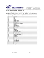
Page 18: ...in5 oscillation circuit Pin6 main relay control Pin7 Power source Pin8 series detect GREEN FUNTION Pin9 CHG ON Pin10 O P V detection Pin11 Input line detection Pin12 Load detection Pin13 RXD Pin14 TXD Pin15 Shutdown Pin16 Buzzer control Pin17 Battery voltage detection Pin18 Inverter PWM signal CPU M3 Pin19 Inverter PWM signal CPU M2 Pin20 Inverter PWM signal CPU M4 Pin21 Inverter PWM signal CPU M1...

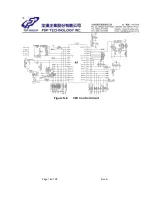
Page 19: ...Page 18 of 28 Rev A Figure S 6 CPU Control Circuit ...

Page 20: ...line mode by switching the relay See Figure W 6 for voltage changes on C1AP during transfer time from line to battery mode CPU pin29 is used to drive signal for RY02 boost relay When the line input voltage is low within boost activated point pin29 sends a high signal to turn on Q05 2SC1815 This will activate the RY02 and UPS will transfer to the Boost mode When the line input voltage increases to ...

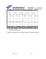
Page 21: ...Page 20 of 28 Rev A CH1 C10 å GND CH2 Output Voltage 1 200V Figure W 6 Output waveform vs voltage change for relay speed up circuitry ...

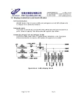
Page 22: ...C start 10 2 Audio alarm The buzzer is controlled by pin16 of CPU When CPU sends a HI signal to buzzer from pin16 buzzer is beeping And CPU sends LOW signal to stop buzzer 10 3 Display Figure S 8 A and Figure S 8 B There are 3 LEDs Vesta 1000 or 6 LEDs Vesta 1500 2000 on the front panel While control button is turned on CPU sends a HI signal to turn on LED Figure S 8 A 3 LEDs Display Circuit ...

Page 23: ...Page 22 of 28 Rev A Figure S 8 B 6 LEDs Display Circuit ...

Page 24: ... CT1AX flows through a full bridge rectifier and R3AX to convert to a voltage signal 0 5 Volts Then CPU can receive output current value of the UPS 11 1 At line boost buck mode The current value multiplies output voltage to get output VA value 11 2 At battery mode Because the power factor of step wave is approximately equal to 1 the current value multiplies 120V 230V output voltage to get output W...

Page 25: ...Page 24 of 28 Rev A 12 I nterface Circuit The interface circuit refer to Figure S 10 USBcommunication and plug play for Windows 95 98 2000 XP NT Figure S 10 USB I nterface Circuit ...

Page 26: ...tems that should be checked are listed below 13 6 1 Are there any connectors or terminals loose 13 6 2 Are there any components burn out or discolored 13 6 3 Especially the power components on the heat sink 13 6 4 Are there any capacitors broken or leakage Check all the components listed above and replace which is abnormal 13 7 Troubleshooting flowchart To prevent from hurting yourself and damagin...

Page 27: ... CPU 27 Check if the value of R83 R82 or R63 R86 is correct 28 Replace R83 R82 or R63 R86 29 Check if Q4 Q9 Q19 or Q30 Q29 Q15 are ok 30 Replace Q4 Q9 Q19 or Q30 Q29 Q15 31 Replace PCB 13 7 2 Line mode examination please refer to flowchart Figure W 8 If battery mode examination is OK then do the line mode examination as below 1 Plug in input power cord at right voltage range Check if main relay RY...

Page 28: ...Page 27 of 28 Rev A Figure W 7 Battery Mode Examination Flowchart ...

Page 29: ...Page 28 of 28 Rev A Figure W 8 Line Mode Examination Flowchart ...

Page 30: ...л т з з любым д бным б м гл т чн я л жб дд ж и Д т в з з в в ии ф мл ни дит нл н з 2 мин ты м нии Д т в и л т вин и тзывы ции и ид и FSP EP 1000 Описание Характеристики ...

Reviews: