22
3.Schematic
FinePix S2 Pro (U/E) SERVICE MANUAL
3.Schematic
3-1.Cautions
<Caution when replaceing chip (leadless) parts.>
* Do not re-use the removed parts, but use new parts.
Be careful that the negativ side of the tantalum capacitors are susceptible to heat.
* Voltage indications are omitted for capacitors other than chemical and tantalum capacitors
with a dielectric strength of 50 V or less.All units are uF (p shows pF).
* Chip resistors without indication are 1/10 W.
* k=1000 , M=1000 k
* Variable resistors and semi-variable resistor are abbreviated the specification of B characteristic.
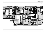
3-2.Basic block name and function explanation
3-3.Description of the Main Block Functions
3-3-1
Overview of the New Technologies
A range of new technologies have been used in this model, and an overview of these is given below.
(1)Improved sensitivity*1 (ISO 1600) and better resolution have been achieved by using a new CCD element that utilizes the
3rd generation Super Honeycom CCD (HA-CCD) structure used in the FinePix S602 but increases the size to APS-film size
(23.3 x 15.6 mm), giving a 6.17 megapixel array with primary color filter.
(This new CCD provides a higher resolution than the FinePix S1 Pro without reducing the S/N ratio, while also allowing
photography at the low ISO 100 sensitivity.)
(2)The optical low-pass filter uses liquid crystal to minimize electrostatic charge, thereby reducing the amount of dust on the
CCD. The surface of the CCD O.LPF has also been given a hard coating to make cleaning easier and more effective.
(3)Image data compression and expansion is performed by the hardware (UCS1; IC306)*2, allowing shorter intervals
between shots at an image size of 4256 pixels x 2848 lines. (The same hardware as the FinePix-S602 is used.)
(4)The camera body used is based on the Nikon F80 camera and takes Nikon's interchangeable lenses.
(5)In response to strong demand from business users, a high-speed IEEE 1394 interface has been provided, along with the
addition of a CCD-RAW format recording function.
*1The Honeycom signal processing roughly doubles the valid number of image pixels, concentrating the data for 4 pixels
into one. This process quadruples the signal level (sensitivity), doubles the S/N (signal-to-noise) ratio and allows shots to
be taken at sensitivity settings up to ISO 1600.
*2The hardware (UCS1; IC306) consists of an M32R core, SRAM and a single chip that provides both the standard peripheral
I/O functions and the functions required by the DSC system. The standard peripheral I/O modules (CPU peripheral I/O
module) comprise an interrupt controller (ICU), system controller (SYSC), DMA controller (DMAC), clock controller (CLKC),
SDRAM controller (SDRAMC), block select controller (BSELC), serial I/O (SIO) interface, USB (USB) interface, multi-function
timer (MFT), watchdog timer (WDT), programmable I/O port (PIO), AD converter (ADC) and DA converter (DAC). In addition,
a JPEG controller (JPEG), signal processor (YCPRO), internal buffer controller (IBFC), AUTO processor (IBFC), media
controller (MEDIA), encoder (ENCD), character generator (CGEN), LCD controller (TFDC), IEEE 1394 interface (EXIO) and
MPEG-2 interface (EXIO) are included as the function modules required for the DSC system (image I/O modules).
Board Name
Block name
Function
CCD PWB UNIT
CCD BLOCK
* CCD output(IC100)
MAIN PWB ASSY
CAM BLOCK
* Analog to digital conversion of CCD output (IC501)
* CCD driver (IC500)
SYSTEM BLOCK
*CAMERA BODY management (IC306)
PROCESS BLOCK
* Video signal processing (IC306)
* USB communication (IC306)
* System control/SW detection management (IC306)
POWER CONT BLOCK
* Power supply management(IC702)
* LCD backlight supply
LCD BLOCK
* LCD control (IC201)
IEEE1394 BLOCK
*IEEE1394 communication (IC1001)
SW PWB ASSY
SW BLOCK
* Operation SW

