23
3.Schematic
FinePix S2 Pro (U/E) SERVICE MANUAL
3-3-2
Block function descriptions
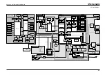
(1) Imaging circuit (CCD BLOCK) (CAM BLOCK)
The analog video signals output from the new APS-size Honeycom CCD (APS-size 6.17-megaixel CCD) are processed
using false-color correction (CDS), optimized spacing (CDS), amplification (AGC) and signal mixing (CDS) in a single CSP-
IC chip (IC501; abbreviated as SCS3A), before being converted (A-D) to 12-bit digital signals. The CSP-IC also incorporates
the "TG/SSG" function, previously provided as a separate IC, onto one chip. The converted digital signals are then sent to the
signal processing IC (abbreviated as UCS1; IC306; CSP).
(2) Image processor (PROCESS BLOCK)
(Input data from the CCD)
The 12-bit digital image data (the section corresponding to 1H) generated by the imaging unit (CCD-CAM BLOCK) is sent to
the signal processing IC (abbreviated as UCS1; IC306), where buffer processing is performed in the IC's internal buffer to
convert the signals to 32-bit (16-bit x 2) data (CCD-RAW data). The converted 32-bit data (CCD-RAW data) is stored in the
16MB SDRAM (IC307 to IC310) via the I/O bus for the image signal processing IC. The image data for each frame (4256
pixels x 2848 lines) is temporarily stored in SDRAM. Also, the 32-bit image data input to the signal processing IC (abbreviated
as UCS1; IC306) is used for additions performed by the AUTO computing unit and then sent to the CAM BLOCK SCS3A
(IC501) so that the optimal AE, AWB and AF values are obtained.
(Recording onto the SSFDC/Microdrive)
The image data stored in the SDRAM (IC307 to IC310) is sent one line at a time to the signal processor IC (IC306; UCS1;
CSP) via the I/O bus in the signal processor IC. In the signal processor, the data is unpacked and the following processes
are called: 16 bit -> 10 bit conversion; preprocessing such as digital clamping, gamma correction, and 10-bit -> 8-bit
conversion for the R, G and B channels; YC processing to convert the 8-bit RGB signals to Y:Cb:Cr=4:2:2, after which the Y,
Cr and Cb 8-bit image data is returned to the internal buffer. In the internal buffer, the 8-bit Y, Cr and Cb signals are sorted
into a data format that facilitates DCT compression before being recorded onto an SSFDC or Microdrive via the JPEG
calculation unit and media controller.
(Image playback from the SSFDC or Microdrive)
The compressed image data on the SSFDC is sent to the signal processing IC (abbreviated as UCS1; IC306) as 8-bit
image data and then sent to SDRAM (IC307 to IC310) via the media control unit, the DMA unit and the internal buffer control
unit. The image data temporarily stored in SDRAM (IC307 to IC310) is then returned to the signal processor IC (abbreviated
as UCS1; IC306) and sent to the signal processor unit via the media controller and JPEG calculation unit. The signal
processor unit performs postprocessing in which the 8-bit Y:Cr:Cb image signals are converted to 8-bit R, G and B signals.
At the same time, the character display signals are superimposed and sent to the LCD BLOCK.
The imaging system adjustment data is stored in F_ROM (IC314).
The 8-bit brightness and color-difference signals processed by the signal processing IC (UCS1; IC306) are D-A converted
in the image signal processing IC encoder unit and the display character signals are superimposed, producing analog
RGB signals. Video (a composite video signal) is also included at the same time in the B component of the RGB signal
output. When the VIDEO terminal is inserted into the camera, a composite video signal is automatically output by the detector.
(3) LCD Controller (LCD BLOCK)
The RGB analog signals output from the image signal processing IC encoder block are sent to the LCD controller IC
(IC201), where they are converted to digital RGB signals. The LCD controller IC also controls the LCD panel gradations at
the same time.
3-3-3.Description of the Power Supply Block Functions
The power supply circuit mounted on the MAIN PWB ASSY board generates a 3.3-volt (IEEE-IC IC1001, UCS1 IC306, SCS3A
IC501, CARD IC201, +16V/-9.0V (CCD power supply)), 7.5-volt (LCD backlight power supply) or 12-volt (LCD panel) supply.
3-3-4.Description of the camera body block functions
The main CPU governs AE calculation and control, AF calculation and control, shutter control, and all communication,
including communication with the DSC unit.
Generation of the power supply and the viewfinder LCD are directly controlled by the SUB CPU.
The interface IC on the MAIN PCB operates as an interface with the AF signals from the linear line sensor (in the CCD FPC)
and sends the AF data to the MPU. It then receives control signals from the MPU and uses these to drive the AF motor.
This IC also controls built-in flash charging and the viewfinder LED.
The camera adjustment parameters are stored in the EEPROM on the MAIN PCB.
The light-metering IC in the pentaprism FPC sends 6-zone light-metering data chronologically to the MPU on the MAIN PCB.
The AF motor drives AF lenses.
The CCD in the CD FPC is a linear line sensor that performs image detection for AF.

