17
3. Schematics
FinePix S5000 Service Manual
3-3. Functions of Primary Blocks.
3-3-1. Technical Outline
The FinePix S5000 incorporates a 1/2.7 inch Fourth Generation Super CCD HR sensor with 3.1 million effective pixels and a
new
signal processing LSI (UCS2, IC206)
. The
signal processing LSI (UCS2, IC206)
is equivalent to the image signal
processing IC (UCS, IC204, CSP) incorporated in the previous FinePix F601, however the new IC permits a dramatic reduction
in the interval between photography and playback. It offers a newly designed super long 10X optical zoom [37-370mm, f2.8-
f8(W)/f3.2-f9(T)]
The S5000 features continuous auto focusing and a low light focus assist lamp. An
[xD picture card]
is adopted as the
recording media.
3-3-2. Functions of Individual Blocks
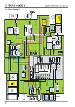
(1) CCD Signal Processing/Picture-taking Blocks (CCD BLOCK and CAMERA BLOCK)
The analog signals output by the CCD (1/2.7 inch Fourth Generation Super CCD HR sensor with 3.1 million effective pixels
[IC1]) undergo color compensation, adaptive interpolation, amplification (ACG) and signal mixing in the
[ACS (IC103)]
CCD
signal processing IC. After that, the signals are converted into 10-bit digital signals and sent to the system LSI
[UCS2 (IC206)]
.
This block has a vertical drive IC (IC101,IC102) for driving the CCD.
(2) Motor Block (MOTOR BLOCK)
Upon receiving commands from operating switches, the
[UCS2 (IC206)]
signal processing LSI manages the motor drive IC
(IC651) so as to control the motors for AF, shutter, zoom and iris.
(3) Image Signal Processing Block (PROCESS BLOCK)
Input Data from the CCD
The 10-bit digital image data (equivalent to 1H) output by the image unit (CCD/CAMERA BLOCK) is sent to the system LSI
[UCS2 (IC206)]
. It is here converted into 16-bit data by the internal buffer of the LSI, and image data of 2816 x 2120 pix per
frame is temporarily stored in the
[IC204,IC205 DRAM (128 Mbit x2)]
of the LSI.
Also, the 10-bit image data input to this LSI is used for calculations by the [auto calculation unit] and sent to the
[ACS (IC103)]
CCD processing IC of the CAMERA BLOCK so as to obtain a suitable AE, AWB and AF.
Recording to the xD picture card
The image data stored in the
[IC204,IC205 DRAM (128 Mbit)]
of the system LSI
[UCS2 (IC206)]
is sent to the signal processing
block one line at a time where it undergoes unpack processing (processing required prior to digital clamping, ( compensation,
10-bit >> 8-bit R/G/B conversion) and YC processing (8-bit digital R/G/B signal >> Y:Cb:Cr = 4:2:2). The 8-bit Y/Cb/Cr data is
then sent to the [internal buffer]. In the
[internal buffer], data is arranged in a format that is easy to convert the 8-bit Y/Cb/Cr data
into DCT. After going through the [JPEG calculation unit] and the [media controller], it is recorded on the xD card.
Play back from the xD picture card
The compressed image data from the xD card is sent to the
[UCS2 (IC206)]
system LSI as 8-bit image data. It is then sent to the
[media control unit] >> [DMA unit] >> [IC204,IC205 DRAM (128 Mbit)] >> [media controller] >> [JPEG calculation unit] >> [signal
processing unit]. The [signal processing unit] does the post-processing of converting the 8-bit Y/Cb/Cr signals into 8-bit R/G/B
signals. At the same time, it weighs the text display signal and displays the text on the LCD UNIT via the [LCD controller].
Camera system adjustment data is stored in the FLASH ROM (IC207).
(4) LCD/EVF UNIT
The digital signal sent from the system LSI
[UCS2 (IC206)]
is sent to the drive IC(IC401) of the LCD UNIT via the processing unit
on the LCD FPC of the LCD UNIT, where [LCD drive] and [LCD panel tonal control] are performed.
(5) Power Supply Block (DCDC BLOCK)
The power supply block is built around the DC IC (IC501). It generates the below power supplies and supplies them to the
individual blocks.
3.3 V
[UCS2 (IC206), ACS (IC103), V-Drv (IC101), FLASH ROM (IC207), STRB IC (IC602),
MOTOR Drv (IC651), PWON IC (IC301), xD Picture Card, MAIN PWB, SUB PWB]
5V
[V-Drv(IC101,MOTOR Drv(IC651),STRB IC (IC602)]
EV3
[Key(IC400),MAIN_PWB, SUB_PWB,PSW_PWB]
A3.3V
[UCS2 (IC206), CLK GEN (IC201), MAIN PWB, LCD]
16 V
[CCD (IC1), OFD(IC101),V Drv (IC102)]
-8 V
[CCD (IC1), V Drv (IC102)]
UNREG
[STRB Block, KEY IC Block]
Summary of Contents for FinePix S5000
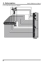
Page 20: ...20 3 Schematics FinePix S5000 Service Manual 3 6 CCD BLOCK Schematic Diagram ...
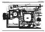
Page 21: ...21 FinePix S5000 Service Manual 3 Schematics 3 7 CAMERA BLOCK Schematic Diagram ...
Page 22: ...22 FinePix S5000 Service Manual 3 Schematics 3 8 PROCESS BLOCK Schematic Diagram ...
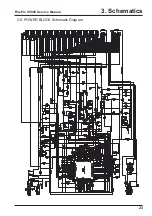
Page 23: ...23 3 Schematics FinePix S5000 Service Manual 3 9 POWER BLOCK Schematic Diagram ...
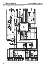
Page 24: ...24 3 Schematics FinePix S5000 Service Manual 3 10 LCD EVF BLOCK Schematic Diagram ...
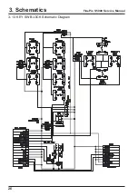
Page 26: ...26 3 Schematics FinePix S5000 Service Manual 3 13 KEY SW BLOCK Schematic Diagram ...
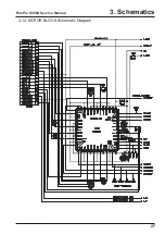
Page 27: ...27 3 Schematics FinePix S5000 Service Manual 3 14 MOTOR BLOCK Schematic Diagram ...
Page 28: ...28 3 Schematics FinePix S5000 Service Manual 3 15 POWER ON BLOCK Schematic Diagram ...
Page 29: ...29 3 Schematics FinePix S5000 Service Manual 3 16 FLASH BLOCK Schematic Diagram ...
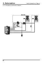
Page 30: ...30 3 Schematics FinePix S5000 Service Manual 3 17 R SW BLOCK Schematic Diagram ...
Page 82: ...26 30 Nishiazabu 2 chome Minato ku Tokyo 106 8620 Japan FUJI PHOTO FILM CO LTD ...


