FinePix S5800/S800 Service Manual
3-2
3. Schematics
Confidential: FUJIFILM Service Center Use Only
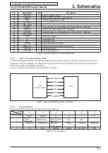
CCDIN
RG
H1-H4
VD
HD
SDATA
SCK
SL
CLI
DOUT
VRB
VRT
PRECISION
TIMING
CORE
SYNC
GENERATOR
PxGA
VGA
ADC
12
2~36 dB
VREF
CLAMP
INTERNAL
REGISTERS
INTERNAL
CLOCKS
CDS
CLAMP
HORIZONTAL
DRIVERS
4
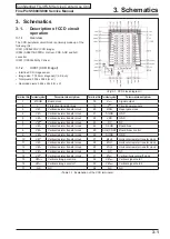
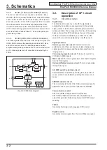
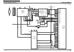
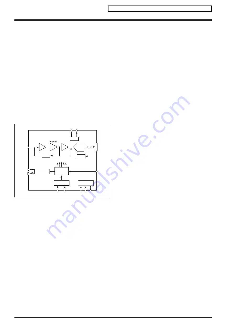
<Fig 3-2. IC905 block diagram>
3-1-3.
IC901 (V driver) and IC905 (H driver)
The H driver and V driver are needed to create the clocks
that drive the CCD (vertical transfer clock, horizontal transfer
clock and the clock for the electronic shutter). IC901 is the V
driver and uses the XV1 to XV15 output from IC101 to create
the vertical transfer clock. XSG is superimposed in IC901
to create a three-value pulse. Also, the XSUB output from
IC101 is the discharge pulse for the electronic shutter. The H
driver is built into IC905 and the H1, H2 and RG clocks are
generated by IC905.
3-1-4.
IC905 (CDS, AGC and A/D converter)
The video signals output from the CCD are input to pin 25 on
IC905. IC905 contains the sampling hold block, AGC block
and A/D converter block. The sampling phase and AGC
amplifier settings are specified based on the serial data from
pin 33. Video signals are A/D converted and output by the
LVDS.
3-2.
Description of CP1 circuit
operation
3-2-1.
Circuit Description
Digital clamp
The black level for each line in the CCD output data is
prepared by calculating an average value for the optically
black portions of the CCD and subtracting that value from
subsequent data. The average value for a line in the optically
black sections of the CCD is taken as the sum of the value
for the previous line multiplied by a coefficient k and the
value for the current line multiplied by a coefficient (k-1).
Signal processor
Gamma (γ) correction circuit:
Gamma correction is
performed so that there is a linear correlation between the
optical input to the camera and the optical output from the
imaging screen.
Color signal generation circuit:
This circuit converts the
CCD data to RGB signals.
Matrix circuit:
This circuit generates Y, R-G and B-G signals
from the RGB signals.
Horizontal/Vertical aperture circuit:
This circuit generates
the aperture signal.
AE, AWB and AF calculation circuit
AE and AWB are calculated by dividing the screen into 64
zones, while AF is calculated by dividing the screen into 6
zones.
SDRAM controller circuit
This circuit outputs the AS, CAS, RAS and address used for
SDRAM control. This circuit also refreshes the SDRAM.
Communication control
SIO: The interface with the 8-bit microprocessor.
SIO for PIO, PWM and LCD: This is 8-bit parallel input/
output that permits individual input/output and PWM output
switching.
TG/SG
Generates the timing and 8-megapixel CCD control.
Digital encoder
Generates chroma signals from the color difference signals.

