FinePix S5800/S800 Service Manual
3-7
3. Schematics
Confidential: FUJIFILM Service Center Use Only
Pin
Signal Name
I/O
Description
49
BATTERY
I
Battery voltage detection
50
VMONIT
I
Main capacitor charging voltage detection
51
TEMP
I
Camera temperature detection
52
NOT USED
-
-
53
NOT USED
-
-
54
SCARD
I
Expansion memory card installation detection signal (L = detected)
55
CARD SW
I
CARD cover switch detection (L = detected)
56
xD CARD
I
Expansion memory card installation detection signal (L = detected)
57
NOT USED
-
-
58
SCK
O
Serial clock output
59
SI
I
Serial data input
60
SO
O
Serial data output
61
CHG ON
O
Flash charging control circuit
62
FLMD0_SY
O
8-bit microprocessor self-programming port
63
PW_ON
I
PW_ON key input
64
LENS_4M
O
LENS clock (4 MHz)
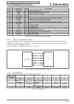
<Table 3-2. 8-bit microprocessor port specifications>
3-5-2.
Internal Communications Paths
The SYA block detects input from the control keys and the status of the camera's circuits and controls the overall camera.
Signals from the various detectors are read by the 8-bit microprocessor as input data and then output to the camera circuit
(ASIC) as operation mode settings information.
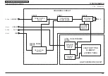
Figure 3-3 shows the 8-bit microprocessor and ASIC connections.
<Fig 3-3. Internal communication path connections>
COMREQ
MAIN RESET
8 bit
microprocessor
ASIC
SDO
SDI
SCK
SREQ
3-5-3.
Key Operations
Refer to the Owner's Manual for information on how to use the keys.
SCAN IN
SCAN OUT
0
1
2
3
4
5
0
AUTO
MOVIE
M
S
P
A
1
Picture
Stabilization
Natural Photo
High-sensitivity
Dual-shot
SP1
SP2
-
2
EVF/LCD
DISP/BACK
Exposure
compensation
WER
F_MODE
OK/MENU
3
UP
LEFT
DOWN
RIGHT
PW_TEST
TEST
<Table 3-3. Key operations>

