


85
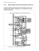
CHAPTER 3 CPU AND CONTROL UNITS
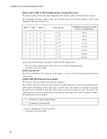
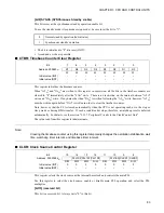
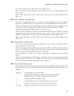
The combination of values written to the bits selects one of the following three types of clock source as
shown below.
•
These bits are initialized to "00
B
" at a reset (INIT).
•
A read and a write are possible.
Notes:
•
The value of the CLKS0 bit (bit8) cannot be changed with the CLKS1 bit (bit9) containing "1".
•
The bits must not be set to any other combination of values.
■
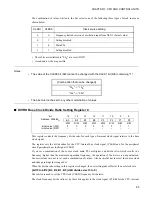
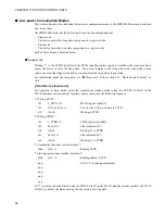
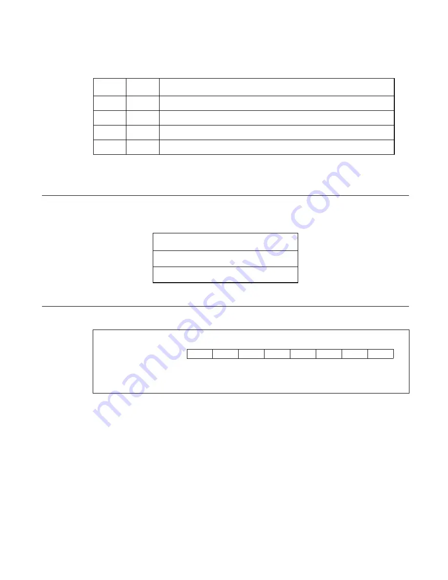
DIVR0: Base Clock Divide Ratio Setting Register 0
This register controls the frequency divide ratio for each type of internal clock signal relative to the base
clock signal.
The register sets the divide ratios for the CPU/internal bus clock signal (CLKB) and for the peripheral
circuit/peripheral bus clock signal (CLKP).
If you set a combination of the source clock, main PLL multiplier, and divide ratio, which results in a
frequency higher than the maximum operating frequency, the operation of the device is not guaranteed.
Use meticulous care not to set such a combination of values. Also be careful not to select the source clock
and change settings in wrong order.
When the divide ratio setting in this register is changed, the new setting takes effect at the next clock rate.
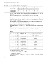
[bit15 to bit12] B3, B2, B1, B0 (clkB divide select 3 to 0)
These bits are used to set the CPU clock (CLKB) frequency divide ratio.
The clock frequency divide ratio set by these bits applies to the clock signal (CLKB) for the CPU, internal
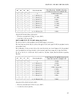
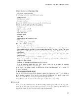
CLKS1
CLKS0
Clock source setting
0
0
Frequency-halved version of oscillation input from X0/X1 (Initial value)
0
1
Setting disabled
1
0
Main PLL
1
1
Setting disabled
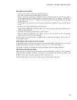
[Combination that can be changed]
"00
B
"
→
"10
B
"
"10
B
"
→
"00
B
"
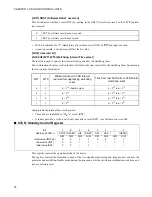
bit
15
14
13
12
11
10
9
8
Address: 000486
H
B3
B2
B1
B0
P3
P2
P1
P0
R/W
R/W
R/W
R/W
R/W
R/W
R/W
R/W
Initial value (INIT)
0
0
0
0
0
0
1
1
Initial value (RST)
×
×
×
×
×
×
×
×
Summary of Contents for FR60Lite
Page 3: ......
Page 5: ......
Page 115: ...100 CHAPTER 3 CPU AND CONTROL UNITS ...
Page 127: ...112 CHAPTER 4 I O PORTS ...
Page 143: ...128 CHAPTER 5 INTERRUPT CONTROLLER ...
Page 155: ...140 CHAPTER 6 EXTERNAL INTERRUPT AND NMI CONTROLLER ...
Page 197: ...182 CHAPTER 9 PPG Programmable Pulse Generator ...
Page 337: ...322 CHAPTER 13 UART ...
Page 417: ...402 CHAPTER 16 DMAC DMA Controller ...
Page 445: ...430 CHAPTER 17 FLASH MEMORY ...
Page 451: ...436 CHAPTER 18 SERIAL PROGRAMMING CONNECTION ...
Page 493: ...478 APPENDIX F Precautions on Handling ...
Page 494: ...479 INDEX INDEX The index follows on the next page This is listed in alphabetic order ...
Page 507: ...492 INDEX ...
Page 509: ......


