


231
CHAPTER 11 MULTIFUNCTIONAL TIMER
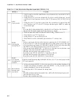
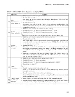
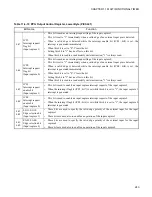
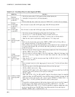
bit11
OTE1:
Output enable bit
•
This bit is used to enable the waveform generator output (RTO1, RTO3, RTO5) to ports.
•
The initial value of this bit is "0".
Note:
When the waveform generator is disabled (the lower of the 16-bit dead timer control register
(DTCR0, DTCR1, DTCR2), TMD2 to TMD0,TMD5 to TMD3, TMD8 to TMD6: bit2 to bit0 =
000
B
), RTO1, RTO3, RTO5 outputs the same value as the output compare.
bit10
OTE0:
Output enable bit
•
This bit is used to enable the waveform generator output (RTO0, RTO2, RTO4) to ports.
•
The initial value of this bit is "0".
Note:
When the waveform generator is disabled (the lower of the 16-bit dead timer control register
(DTCR0, DTCR1, DTCR2), TMD2 to TMD0,TMD5 to TMD3, TMD8 to TMD6: bit2 to bit0 =
000
B
), RTO0, RTO2, RTO4 outputs the same value as the output compare.
bit9
OTD1:
Output level bit
•
This bit is used to change a pin output level of the output compare 1, 3, 5 (RT1, RT3, RT5).
•
The initial value of the compare pin output is "0".
•
Before data is written, be sure to stop the compare operation. The read value of this bit
indicates the output compare value of RT1, RT3, RT5.
bit8
OTD0:
Output level bit
•
This bit is used to change a pin output level of the output compare 0, 2, 4 (RT0, RT2, RT4).
•
The initial value of the compare pin output is "0".
•
Before data is written, be sure to stop the compare operation. The read value of this bit
indicates the output compare value of RT0, RT2, RT4.
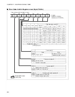
Table 11.4-4 Compare Control Register, Upper Byte (OCSH1, OCSH3, OCSH5) (2 / 2)
Bit Name
Function
Summary of Contents for FR60Lite
Page 3: ......
Page 5: ......
Page 115: ...100 CHAPTER 3 CPU AND CONTROL UNITS ...
Page 127: ...112 CHAPTER 4 I O PORTS ...
Page 143: ...128 CHAPTER 5 INTERRUPT CONTROLLER ...
Page 155: ...140 CHAPTER 6 EXTERNAL INTERRUPT AND NMI CONTROLLER ...
Page 197: ...182 CHAPTER 9 PPG Programmable Pulse Generator ...
Page 337: ...322 CHAPTER 13 UART ...
Page 417: ...402 CHAPTER 16 DMAC DMA Controller ...
Page 445: ...430 CHAPTER 17 FLASH MEMORY ...
Page 451: ...436 CHAPTER 18 SERIAL PROGRAMMING CONNECTION ...
Page 493: ...478 APPENDIX F Precautions on Handling ...
Page 494: ...479 INDEX INDEX The index follows on the next page This is listed in alphabetic order ...
Page 507: ...492 INDEX ...
Page 509: ......


