


286
CHAPTER 11 MULTIFUNCTIONAL TIMER
●
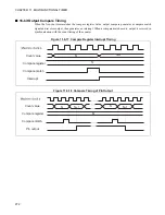
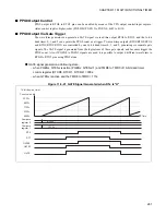
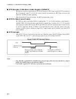
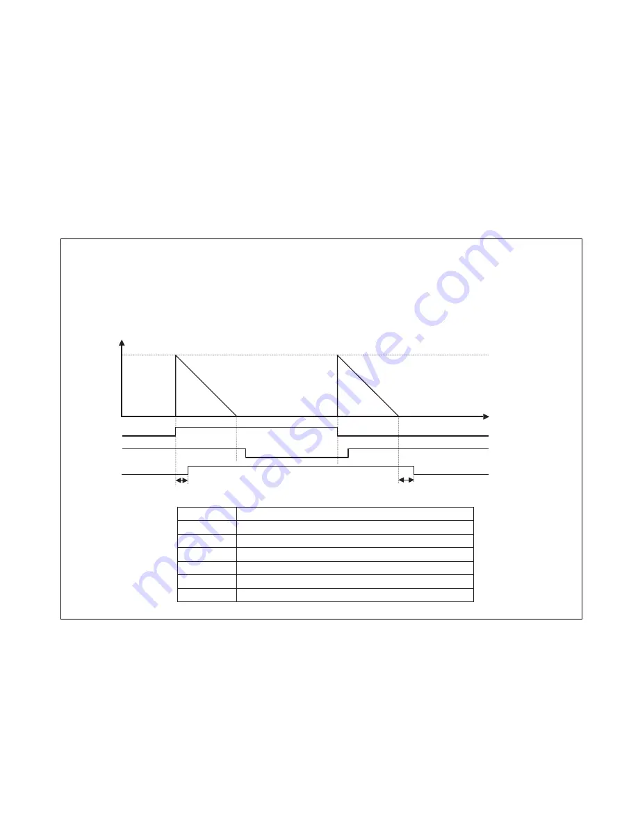
This non-overlapping signal is generated via reverse-polarity RT1, RT3, and RT5 (16-bit dead timer
control register (DTCR0, DTCR1, and DTCR2) TMD8 to TMD0 (higher-order bits are 10 to 8; lower-
order bits are 2 to 0) = 100
B
).
When the DTCR0, DTCR1, and DTCR2 register's DMOD2 to DMOD0 (higher-order bit is 15; lower-order
bit is 7) selects the non-overlapping signal with a value of 1 (reverse polarity), a delay equivalent to the
non-overlap time set in the 16-bit dead timer register (TMRRH0 to TMRRH2, TMRRL0 to TMRRL2) is
applied. This delay is applied to the rising edge or falling edge of the RT1, RT3, and RT5. If the RT1, RT3,
and RT5 pulse width is less than the specified non-overlap time, the 16-bit dead timer starts counting down
again from the next RT edge TMRRH0 to TMRRH2 and TMRRL0 to TMRRL2 value.
Figure 11.6-25 Non-overlap Signal Generated by RT1, RT3, and RT5 of Inverted Polarity
Pin name
Output signal
RTO0 (U)
Delayed inverted signal is applied at rising edge of RT1.
RTO2 (V)
Delayed inverted signal is applied at rising edge of RT3.
RTO4 (W)
Delayed inverted signal is applied at rising edge of RT5.
RTO1 (X)
Delayed signal is applied at falling edge of RT1.
RTO3 (Y)
Delayed signal is applied at falling edge of RT3.
RTO5 (Z)
Delayed signal is applied at falling edge of RT5.
<Register setting>
TCDTH, TCDTL
: XXXX
H
OCCPH0 to OCCPH5, OCCPL0 to OCCPL5 : XXXX
H
(Compare value)
TCCSH, TCCSL
: XXXXXXXX X0X0XXXX
B
OCSH0 to OCSH5, OCSL0 to OCSL5
: -XX1XXXX XXXXXX11
B
CPCLRH, CPCLRL
: XXXX
H
(Setting of cycle)
DTCR0 to DTCR2
: 1XXXX100
B
TMRRH0 to TMRRH2, TMRRL0 to TMRRL2 : XXXX
H
(Setting of non-overlap timing)
SIGCR1
: XXXXXXXX
B
(Setting of DTTI input and 16-bit dead timer count clock)
Note: Be sure to set according to "X" operation.
RTO0(U)
Time
TMRR0 set
value
Count value
RTO1(X)
16-bit dead timer 0
RT1
2 machine cycle
2 machine cycle
Summary of Contents for FR60Lite
Page 3: ......
Page 5: ......
Page 115: ...100 CHAPTER 3 CPU AND CONTROL UNITS ...
Page 127: ...112 CHAPTER 4 I O PORTS ...
Page 143: ...128 CHAPTER 5 INTERRUPT CONTROLLER ...
Page 155: ...140 CHAPTER 6 EXTERNAL INTERRUPT AND NMI CONTROLLER ...
Page 197: ...182 CHAPTER 9 PPG Programmable Pulse Generator ...
Page 337: ...322 CHAPTER 13 UART ...
Page 417: ...402 CHAPTER 16 DMAC DMA Controller ...
Page 445: ...430 CHAPTER 17 FLASH MEMORY ...
Page 451: ...436 CHAPTER 18 SERIAL PROGRAMMING CONNECTION ...
Page 493: ...478 APPENDIX F Precautions on Handling ...
Page 494: ...479 INDEX INDEX The index follows on the next page This is listed in alphabetic order ...
Page 507: ...492 INDEX ...
Page 509: ......


