310
CHAPTER 13 UART
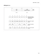
■
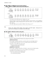
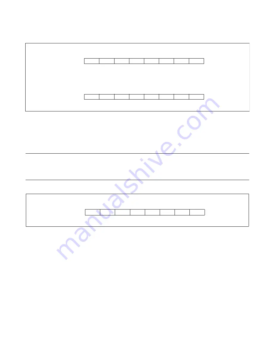
SIDR: SIDR0 to SIDR2 (Serial Input Data Register)
SODR: SODR0 to SODR2 (Serial Output Data Register)
These registers are data buffer registers for sending and receiving.
If the data length is seven bits, bit7 (D7) of SIDR and SODR contains invalid data. Accessing SIDR and
SODR when BDS=1 switches the high-order and low-order data on the bus. As a result, it appears that bit0
(D0) is ignored.
Write to the SODR register only while the TDRE bit of the SSR register is "1".
Note:
Writing to the register with this address means writing to the SODR register. Reading from the
register with this address means reading from the SIDR register.
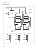
■
SSR: SSR0 to SSR2 (Serial Status Register)
The SSR is configured from flags that indicate the operating status of the UART.
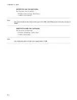
[bit7] PE (Parity Error):
This bit, which is an interrupt request flag, is set when a parity error occurs during reception.
To clear the flag when it has been set, write "0" to the REC bit (bit10) of the SCR register.
If the PE bit is set, the SIDR data becomes invalid.
0: No parity error has occurred. [Initial value]
1: A parity error has occurred.
[bit6] ORE (Over Run Error):
This bit, which is an interrupt request flag, is set when an overrun error occurs during reception.
To clear the flag when it has been set, write "0" to the REC bit of the SCR register.
If the ORE bit is set, the SIDR data becomes invalid.
0: No overrun error has occurred. [Initial value]
1: An overrun error has occurred.
SIDR
Address
bit7
bit6
bit5
bit4
bit3
bit2
bit1
bit0
Initial value
ch0 000061
H
ch1 000069
H
ch2 000071
H
D7
D6
D5
D4
D3
D2
D1
D0
Undefined
R
R
R
R
R
R
R
R
SODR
Address
bit7
bit6
bit5
bit4
bit3
bit2
bit1
bit0
Initial value
ch0 000061
H
ch1 000069
H
ch2 000071
H
D7
D6
D5
D4
D3
D2
D1
D0
Undefined
W
W
W
W
W
W
W
W
SSR
Address
bit7
bit6
bit5
bit4
bit3
bit2
bit1
bit0
Initial value
ch0 000060
H
ch1 000068
H
ch2 000070
H
PE
ORE
FRE
RDRF
TDRE
BDS
RIE
TIE
00001000
B
R
R
R
R
R
R/W
R/W
R/W
Summary of Contents for FR60Lite
Page 3: ......
Page 5: ......
Page 115: ...100 CHAPTER 3 CPU AND CONTROL UNITS ...
Page 127: ...112 CHAPTER 4 I O PORTS ...
Page 143: ...128 CHAPTER 5 INTERRUPT CONTROLLER ...
Page 155: ...140 CHAPTER 6 EXTERNAL INTERRUPT AND NMI CONTROLLER ...
Page 197: ...182 CHAPTER 9 PPG Programmable Pulse Generator ...
Page 337: ...322 CHAPTER 13 UART ...
Page 417: ...402 CHAPTER 16 DMAC DMA Controller ...
Page 445: ...430 CHAPTER 17 FLASH MEMORY ...
Page 451: ...436 CHAPTER 18 SERIAL PROGRAMMING CONNECTION ...
Page 493: ...478 APPENDIX F Precautions on Handling ...
Page 494: ...479 INDEX INDEX The index follows on the next page This is listed in alphabetic order ...
Page 507: ...492 INDEX ...
Page 509: ......

