420
CHAPTER 17 FLASH MEMORY
17.5
Automatic Algorithm Execution Status
Flash memory is provided with hardware to notify the internal operation status of flash
memory and the completion of the operation to the outside of the flash memory for
executing write/erase operations in the automatic algorithm. One is a ready/busy signal
and the other is a hardware sequence flag.
■
Ready/Busy Signal (RDY/BUSY)
The flash memory has the ready/busy signal in addition to the hardware sequence flag for indicating
whether the internal automatic algorithm is running or completed. This ready/busy signal is connected to
the flash memory interface circuit, and it can be read as the RDY bit of the flash memory status register.
Also, by starting this ready/busy signal, it can generate an interrupt request to the CPU (see "17.1
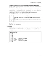
When the read value of the RDY bit is "0", the flash memory is executing a write or erase operation, where
new write and erase commands are not accepted. When the value of the RDY bit is "1", the flash memory
is in read/write state or in erase operation wait state.
■
Hardware Sequence Flag
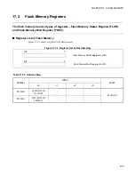
Hardware sequence flag can be obtained as data by reading an arbitrary address (or odd number address in
byte access) of the flash memory during automatic algorithm operation. In the data, valid bits are five bits
and each of them indicates the status of the automatic algorithm. Figure 17.5-1 shows the structure of the
hardware sequence flag.
Figure 17.5-1 Structure of the Hardware Sequence Flag
The hardware sequence flag becomes invalid in FR-CPU ROM mode. Always use FR-CPU programming
mode and read only in halfwords or bytes.
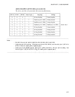
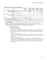
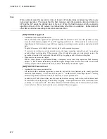
Table 17.5-1 shows a hardware sequence flag status list.
During hardware read
15
8 7
0
←
Bit No.
(Undefined)
Hardware sequence flag
7
0
←
Bit No.
During byte read (only for odd address)
Hardware sequence flag
During halfword and byte access
7
6
5
4
3
2
1
0
←
Bit No.
DPOLL
TOGGLE
TLOVER
Undefined
SETIMR
TOGGL2
Undefined
Undefined
Summary of Contents for FR60Lite
Page 3: ......
Page 5: ......
Page 115: ...100 CHAPTER 3 CPU AND CONTROL UNITS ...
Page 127: ...112 CHAPTER 4 I O PORTS ...
Page 143: ...128 CHAPTER 5 INTERRUPT CONTROLLER ...
Page 155: ...140 CHAPTER 6 EXTERNAL INTERRUPT AND NMI CONTROLLER ...
Page 197: ...182 CHAPTER 9 PPG Programmable Pulse Generator ...
Page 337: ...322 CHAPTER 13 UART ...
Page 417: ...402 CHAPTER 16 DMAC DMA Controller ...
Page 445: ...430 CHAPTER 17 FLASH MEMORY ...
Page 451: ...436 CHAPTER 18 SERIAL PROGRAMMING CONNECTION ...
Page 493: ...478 APPENDIX F Precautions on Handling ...
Page 494: ...479 INDEX INDEX The index follows on the next page This is listed in alphabetic order ...
Page 507: ...492 INDEX ...
Page 509: ......

