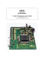
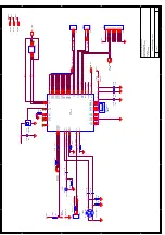
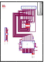
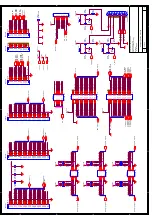
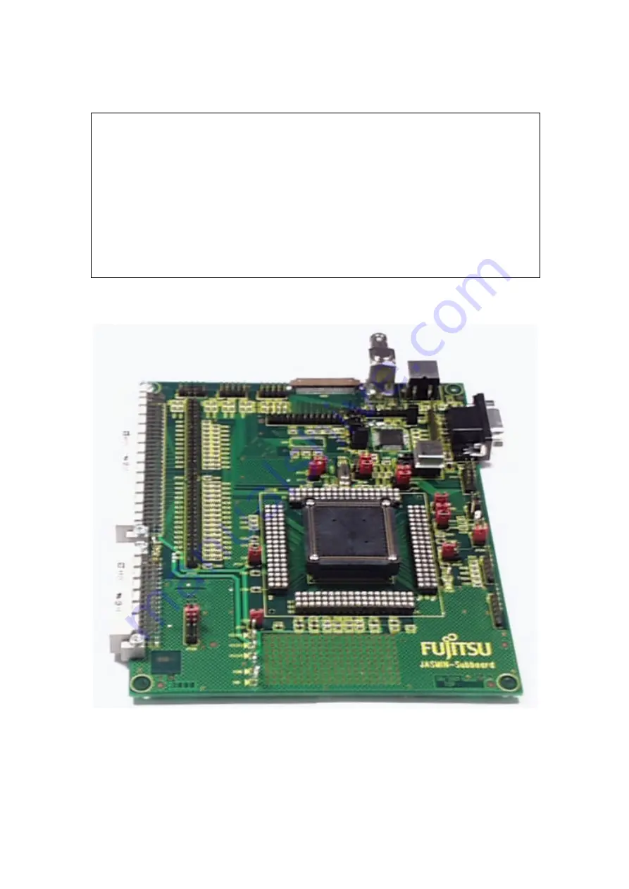
background image


JASMINE- 

Subboard 

Documentation 


Fujitsu Microelectronics Europe GmbH


Am Siebenstein 6-10 

63303 Dreieich-Buchschlag, Germany 


Summary of Contents for JASMINE

Page 1: ...JASMINE Subboard Documentation Fujitsu Microelectronics Europe GmbH Am Siebenstein 6 10 63303 Dreieich Buchschlag Germany ...

Page 2: ...2 History Revision Date Comment V1 0 07 03 01 New Document ...

Page 3: ... defect Fujitsu Microelectronics Europe GmbH entire liability and the customer s exclusive remedy shall be at Fujitsu Microelectronics Europe GmbH sole discretion either return of the purchase price and the license fee or replacement of the Product or parts thereof if the Product is returned to Fujitsu Microelectronics Europe GmbH in original packing and without further defects resulting from the ...

Page 4: ...ocumentation and software on a CD ROM For documentation or software updates please refer to our web site www fujitsu fme com Fujitsu reserves the right to make changes to its products or to discontinue any semiconductor product or service without notice 07 03 01 V1 0 ...

Page 5: ... CPU Modul interface 3 Jumpers This chapter describes all jumpers which can be modified on the evaluation board The default setting is shown with a gray shaded area All jumpers and switches are named directly on the board by its meaning so it is very easy to set the jumpers according to the features 3 1 Power Supply Voltage JP205 JP206 JP207 Jumper setting Description ON closed Core supply 2V5 2V5...

Page 6: ...mine devices can be join one chip select The size and location of configuration for every Jasmine is fixed The size is set to 64 kByte for every Jasmine and the location are specified by Mode Jumpers JP201 JP202 Jasmine number JP202 JP201 Jasmine 0 2 3 2 3 Jasmine 1 2 3 1 2 Jasmine 2 1 2 2 3 Mode1 0 Jasmine 3 1 2 1 2 Jasmine can also act as a 16Bit device from MCU s point of view The data mode can...

Page 7: ...t of the MCU to execute a software Reset JP212 Description 1 2 Software Reset Reset 2 3 VGC Reset 3 6 SPB Interface JP209 JP215 JP209 Description ON closed SPB needs pull up for operation SPB_BUS OFF open SPB no operation JP215 Description ON closed Probe clock enable SPB_TST clock debug output OFF open Probe clock not enable 3 7 RDY JP213 Tristate enable for RDY RDY can be driven with a pull up i...

Page 8: ...2 Description 1 2 Chip enable connected with VCC VIC enable 2 3 Chip enable connected with PortS0 MCU JP301 Description GND closed 0 48h for write 49h for read I2 C Bus slave address select VCC open 1 4Ah for write 4Bh for read JP305 Description 1 2 HS connected with VREF GDC Video Scaler Vertical Reference 2 3 VS connected with VREF GDC JP306 Description 1 2 Video flag from ext video decoder Vide...

Page 9: ...tput signal Cref Clock reference output HS Horizontal sync output signal VS Vertical sync output signal GPSW General purpose switch output RES out Reset output active low VIC Signals JP401 BUS_VCS_D7 0 Video scaler data input VSC_CLKV Video scaler clock LVDS connector JP402 Signals for LVDS connector Display Signals JP501 DIS_PIXCLK Display pixel clock A_RED Analog red A_GREEN Analog green A_BLUE ...

Page 10: ...l for bus transfer ULB_RDX Read enable for ULB data bus ULB_WRX3 0 Write enable for ULB data bus ULB_CLK ULB interface clock ULB_CS Chip select ULB_DREQ DMA request signal ULB_DACK DMA acknowledge signal For more information please look at the Hardware Manual of the Jasmine graphic controller and the Data Sheet of the Video Input Processor SAA7111A ...

Page 11: ...11 4 Schematics and Drawings ...

Page 12: ...B5 8 B 1754 8 B 5 4 8 B 02 02 02 02 95 96 B 17 96 B 3 96 B 9 96 B9 7 96 B95 96 B 96 B 96 B 96 B 96 B 96 B 96 B 96 B 96 B 9 6B 96 B 96 B 96 B 96 B 96 B 96 B 7 67 5 6 7 B952 93 26 B 1 26 B287 6B 6B96 1 6B 6 1 6B3 6B 6B 6B 6B 6B 6B 6B 6B 6B 6B 6B 6B 6B 6B 6B 6B 6B 6B 6B 6B 6B 6B 6B 6B 6B95 9 9 9 9 9 9 9 9 9 9 9 9 9 9 9 9 9 9 9 9 9 9 9 9 9 9 9 B2 B 1 7 B 7 B 7 B9 B9 B 8 B966 B966 B9 B 5 1 B966 B9 B5 B...

Page 13: ...6B96 B 86B96 B 86B96 B 86B96 B 86B96 B 86B96 B 86B96 B 86B96 B 86B96 B 86B96 B 86B96 B 86B96 B 5 96 B 17 96 B 17 6 B9 96 9UHI 9 9 9 9 9 9 9 9 9 9 9 9 3 5 5 5 Q 3 5 Q 8 6 932 932 932 932 932 932 932 932 932 932 932 932 932 932 932 932 Q F Q F 9VV 9GG 9VV 9GG 9VVV 9GG 9VV 9GG 9VV 9GG 9VV 9VV 9GG 9VV 9GG 9VV 9GG B6 B6 RXW 9UHI UHI 7 7 UHI 7 2 7 706 7567 7 5 6 6 576 576 96 36 57 B6 Q 5 5 5 N 0 5 N Q P...

Page 14: ...86B 6B 86B 6B 86B 6B 86B 6B 86B 6B 86B 6B 86B 6B 86B 6B 86B 6B 86B 6B 86B 6B 86B 6B 86B 6B 86B 6B 86B 6B 86B 6B 86B 6B 6B 6 1 6B96 1 6B3 6B95 9 9 9 9 9 9 9 9 9 9 6 6 7 7 287 7 287 1 7 287 7 86 1 7 287 7 287 1 7 287 6 7 287 7 287 1 7 287 86 86 6 86 6 7 287 7 287 1 7 287 86 9 7 7 287 7 287 1 7 287 7 5 N 3 5 Q Q Q 527 5h1 8 8 61 9 6 9 9 9 3 9 9 69 1 1 1 1 1 3 1 3 1 9 6 1 9 6 1 9 6 1 1 1 2873 2870 6 7...

Page 15: ...B 6B 86B 6B 86B 6B 86B 6B 86B 6B 86B 6B 86B 6B 86B 86B 86B 86B 86B 86B 86B 86B 86B 86B 9FF 9 86B 86B 86B 86B 86B 86B 86B 86B 86B 86B 86B 86B 86B 86B 86B 86B 86B 86B 86B 86B 86B 86B 86B 86B 86B 86B 86B 86B 86B 86B 86B 86B 86B 86B 86B 86B 86B 3RUW6 9FF 9 B B 517 B B QWHUUXSWB B8 57B5 B 54 B6 B6 B8 57B7 B8 57B 2 6B 6 6 6 6 6 6 6 9FF 9 5 1 5 8 1 1 1 1 1 9 9 9 9 9 9 9 9 9 9 9 9 9 9 9 9 9 9 9 9 9 9 9 9 ...

Reviews: