background image

Fujitsu ASSP Product

2/14

Power Management 

MB39C026 Evaluation Board

The  MB39C026  is  a  two  channels  power  supply  IC.  It  consists  of  one  channel 

DC/DC Converter and one channel LDO regulator. The DC/DC converter has fast 

line  transient  response  and  load  regulation  with  current  mode  control  topology. 

Moreover,  the  integrated  LDO  provides  an  auxiliary  output  supply for  noise 

sensitive circuit. 

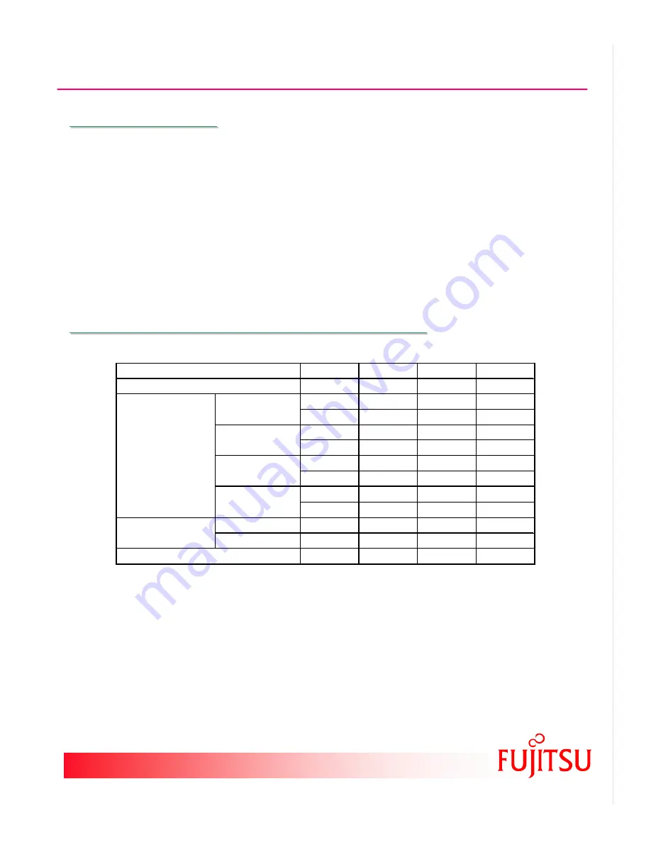
2. Evaluation Board Specification

2. Evaluation Board Specification

1. Description

1. Description

* CH1 Remark:

Maximum  Output  voltage  is  limited  by  the  input  voltage  (VIN).  The  maximum 

voltage CH1 could reach is 0.5V less than VIN.

# CH2 Remark: 

The  CH2 output  voltage  is  limited  by  input  voltage  (VIN).  The  CH2  dropout  of 

MB39C026G is Vdrop. Thus the minimum input voltage should be Vdrop above 

the CH2 output. Vdrop is 0.2V(Typ).

Min.

Typ.

Max.

3.2

3.7

5.5

CH1

0.8

1.2

5*

CH2

3.3#

CH1

0.8

1.2

5*

CH2

2.85

CH1

0.8

1.2

5*

CH2

1.8

CH1

0.8

1.8

5*

CH2

1.2

CH1

0

-

600

CH2

0

-

300

-

2.0

-

Oscillation Frequency

Output Current

Parameter

Input Voltage

MB39C026G

MB39C026J

MB39C026L

MB39C026N

Output Voltage

Summary of Contents for MB39C026

Page 1: ...Evaluation Board Rev 1 0E June 2008 MB39C026 MB39C026 Evaluation Board Manual Evaluation Board Manual SON SON 10 10 MB39C022 MB39C022 EVB03 EVB03 MB39C026 and MB39C022 share the same evaluation board MB39C026 and MB39C022 share the same evaluation board ...

Page 2: ...aluation Board Specification 1 Description 1 Description CH1 Remark Maximum Output voltage is limited by the input voltage VIN The maximum voltage CH1 could reach is 0 5V less than VIN CH2 Remark The CH2 output voltage is limited by input voltage VIN The CH2 dropout of MB39C026G is Vdrop Thus the minimum input voltage should be Vdrop above the CH2 output Vdrop is 0 2V Typ Min Typ Max 3 2 3 7 5 5 C...

Page 3: ...ach output are as follows MB39C026G VO1 1 2V VO2 3 3V POR VIN MB39C026J VO1 1 2V VO2 2 85V POR VIN MB39C026L VO1 1 2V VO2 1 8V POR VIN MB39C026N VO1 1 8V VO2 1 2V POR VIN 3 Terminal information 3 Terminal information Pin Name Description VIN Input voltage terminal PGND Ground terminal for power supply VO1 CH1 DC DC converter output terminal PGND1 Ground terminal for CH1 DC DC converter VO2 CH2 LDO...

Page 4: ...Fujitsu ASSP Product 4 14 Power Management MB39C026 Evaluation Board 5 Evaluation Board Layout 5 Evaluation Board Layout MB39C022 EVB03 Rev 1 0 Top View Top Side Silkscreen Bottom Side Silkscreen ...

Page 5: ...Fujitsu ASSP Product 5 14 Power Management MB39C026 Evaluation Board Board Layout Top View Top Side Metal Bottom Side Metal MB39C022 EVB03 Rev 1 0 ...

Page 6: ...EN1 EN2 JP1 JP2 For VO1 1 2V R5 1 300k For VO1 1 8V R5 1 499k Count Designator Description Part Number Manufacturer 1 U1 Power IC MB39C026 Fujitsu 2 C1 C2 Capacitor 4 7uF 10V C1608JB1A475K TDK 1 C3 Capacitor 22pF 50V C1608CH1H220J TDK 2 C4 C5 Capacitor 1uF 16V C1608JB1C105K TDK 1 L1 Inductor 2 2uH RDC 76m VLF4012AT 2R2M1R5 TDK 3 R1 R2 R3 Resistor 1M 1 Resistor 300k 1 for 1 2Voutput Resistor 499k 1...

Page 7: ...to start the LDO converter VO2 R2 pull down EN2 to GND and disable VO2 if EN2 has no input Power On Reset POR R3 and R4 are the pull up resistors for POR Pin 4 A 1M resistor is required to placed at either R3 or R4 When R3 has a 1M resistor and R4 is open the POR will be connected VIN When R4 has a 1M resistor and R3 is open the POR pin will be connected to VO1 By default only R3 require a 1M resi...

Page 8: ... A VO1 Output Voltage V VIN 3 7V VIN 4 3V VIN 5 5V CH1 Efficiency 0 10 20 30 40 50 60 70 80 90 0 001 0 01 0 1 1 IO1 Load Current A Efficiency VIN 3 7V VIN 4 3V VIN 5 5V CH1 Test Condition EN1 VIN EN2 0V VO1 1 8V C1 C2 4 7uF CH1 Test Condition EN1 VIN EN2 0V VO1 1 8V C1 C2 4 7uF CH1 Efficiency 0 10 20 30 40 50 60 70 80 90 100 0 001 0 01 0 1 1 IO1 Load Current A Efficiency VIN 3 7V VIN 4 3V VIN 5 5V...

Page 9: ...t Condition EN1 EN2 VIN VO1 1 8V IO1 20mA C1 C2 4 7uF VO2 3 3V IO2 150mA C4 C5 1uF CH1 Line Regulation 1 1 1 12 1 14 1 16 1 18 1 2 1 22 1 24 1 26 1 28 1 3 3 2 3 7 4 2 4 7 5 2 VIN Input Voltage V VO1 Output Voltage V IO1 0mA IO1 300mA IO1 600mA VLx 5V div ILx 100mA div VO1 20mV div VO2 20mV div 500ns div VLx 5V div ILx 100mA div VO1 20mV div VO2 20mV div 5us div CH1 Line Regulation 1 7 1 72 1 74 1 ...

Page 10: ...26 3 28 3 3 3 32 3 34 3 36 3 38 3 4 0 0 1 0 2 0 3 IO2 Load Current A VO 2 O utput Voltage V VIN 3 7V VIN 4 3V VIN 5 5V CH2 Load Regulation 1 7 1 72 1 74 1 76 1 78 1 8 1 82 1 84 1 86 1 88 1 9 0 0 1 0 2 0 3 IO2 Load Current A VO2 Output Voltage V VIN 3 7V VIN 4 3V VIN 5 5V CH2 Load Regulation 1 1 1 12 1 14 1 16 1 18 1 2 1 22 1 24 1 26 1 28 1 3 0 0 1 0 2 0 3 IO2 Load Current A VO2 Output Voltage V VI...

Page 11: ...2 87 2 89 2 91 2 93 2 95 3 2 3 7 4 2 4 7 5 2 VIN Input Voltage V VO2 Output Voltage V IO2 0mA IO2 120mA IO2 300mA CH2 Line Regulation 3 2 3 22 3 24 3 26 3 28 3 3 3 32 3 34 3 36 3 38 3 4 3 6 4 1 4 6 5 1 VIN Input Voltage V VO2 Output Voltage V IO2 0mA IO2 120mA IO2 300mA CH2 Line Regulation 1 7 1 72 1 74 1 76 1 78 1 8 1 82 1 84 1 86 1 88 1 9 3 2 3 6 4 4 4 4 8 5 2 VIN Input Voltage V VO2 Output Volt...

Page 12: ...1 2V IO2 100mA Cin 0 Power Supply Rejection Ratio IO2 100mA 80 70 60 50 40 30 20 10 0 10 100 1000 10000 100000 1000000 Freq Hz PSRR dB VIN 3 7V VIN 4 3V Power Supply Rejection Ratio IO2 100mA 80 70 60 50 40 30 20 10 0 10 100 1000 10000 100000 1000000 Freq Hz P S R R d B Vin 3 7V Vin 4 3V Power SupplyRejection Ratio IO2 100mA 80 70 60 50 40 30 20 10 0 10 100 1000 10000 100000 1000000 Freq Hz P S R ...

Page 13: ...V VO1 1 2V C1 C2 4 7uF IO1 250mA VO2 3 3V C4 C5 1uF IO2 150mA VIN 2V div VO1 2V div VO2 2V div IO1 250mA IO2 150mA POR 2V div VO1 2V div VO2 2V div IO1 250mA IO2 150mA CH1 Load Transients CH2 Load Transients Startup Waveform POR Waveform 50us div 20ms div IO1 500mA div VO1 100mV div VO2 20mV div IO1 10mA to 400mA IO2 150mA 20us div IO2 200mA div VO2 20mV div VO1 20mV div IO2 10mA to 250mA IO1 250m...

Page 14: ...old devices etc CAUTION Customers considering the use of our products in special applications where failure or abnormal operation may directly affect human lives or cause physical injury or property damage or where extremely high levels of reliability are demanded such as aerospace systems atomic energy controls sea floor repeaters vehicle operating controls medical devices for life support etc ar...

Reviews: