


101
CHAPTER 4 RESET
4.4
Resetting
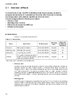
After the cancellation of a reset, a read from operation of mode data and the reset
vector can be selected by setting the mode pin to perform mode fetching. Mode
fetching determines the CPU operation mode and the start address of execution after
the end of a reset. When the power is turned on or when the system is returned from
the stop-mode by a reset, perform mode fetching after the end of the oscillation
stabilization wait time.
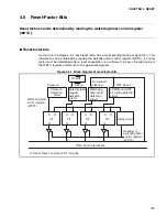
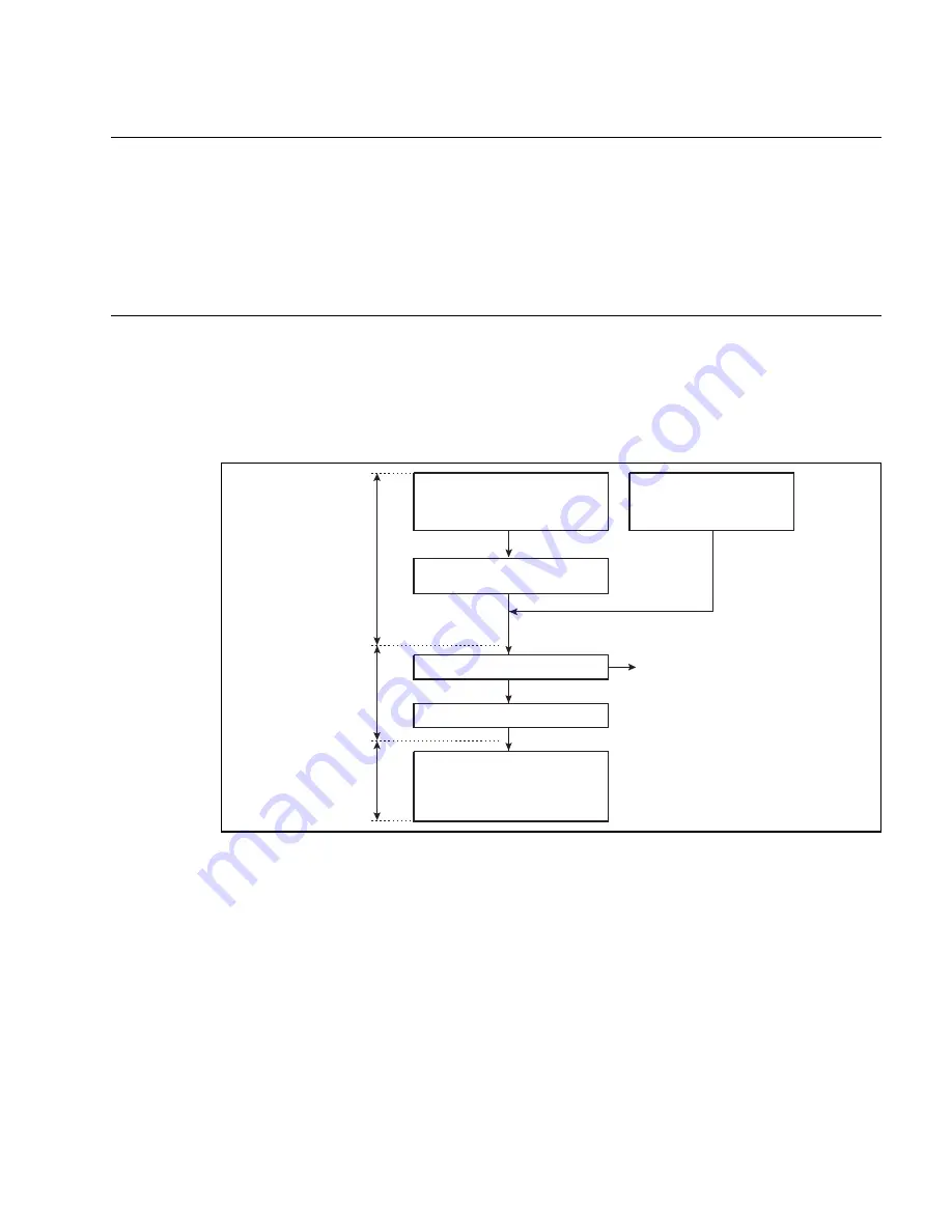
■
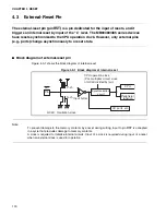
Overview of resetting
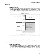
Figure 4.4-1 shows the flow of resetting.
Figure 4.4-1 Flow of resetting
■
Mode pins
Mode pins (MD2 to MD0) specify a method to fetch reset vectors and mode data. A reset vector
and mode data are fetched in a sequence for resetting. Refer to Section "7.2 Mode Pins (MD2
to MD0)", for details of the mode pins.
■
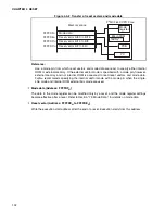
Mode fetch
After a reset is canceled, the CPU transfers the reset vectors and mode data to the applicable
registers in the CPU core. The reset vectors and mode data are allocated to four bytes, namely
FFFFDC
H
to FFFFDF
H
. Upon a reset cancellation, the CPU immediately outputs these
addresses to a bus and fetches reset vectors and mode data. During mode fetching, the CPU
starts processing from the address specified by the reset vector.
Figure 4.4-2 shows transfer of reset vectors and mode data.
Power-on reset
Stop mode
Sub clock mode
Fetch of instruction code
from addresses indicated
by a reset vector, and
execution of instruction
Reset state to wait for
stable oscillation
Fetch of mode data
Fetch of reset vector
Pin state and function changes
related to external bus mode
Reset in progress
Mode fetching
(reset)
Normal operation
(run state)
External reset
Software reset
Watchdog timer reset
Summary of Contents for MB90480 Series
Page 2: ......
Page 4: ......
Page 10: ...vi ...
Page 128: ...106 CHAPTER 4 RESET ...
Page 174: ...152 CHAPTER 6 LOW POWER CONSUMPTION MODE ...
Page 198: ...176 CHAPTER 7 MODE SETTING ...
Page 220: ...198 CHAPTER 9 TIMEBASE TIMER ...
Page 238: ...216 CHAPTER 11 WATCH TIMER ...
Page 280: ...258 CHAPTER 12 16 BIT INPUT OUTPUT TIMER ...
Page 406: ...384 CHAPTER 17 8 10 BIT A D CONVERTER ...
Page 478: ...456 CHAPTER 20 CHIP SELECTION FACILITY ...
Page 494: ...472 CHAPTER 21 ADDRESS MATCH DETECTION FUNCTION ...
Page 498: ...476 CHAPTER 22 ROM MIRROR FUNCTION SELECTION MODULE ...
Page 526: ...504 CHAPTER 23 2M 3M BIT FLASH MEMORY ...
Page 536: ...514 CHAPTER 24 EXAMPLES OF MB90F481B MB90F482B MB90F488B MB90F489B SERIAL PROGRAMMING ...
Page 570: ...548 CHAPTER 25 PWC TIMER ONLY MB90485 SERIES ...
Page 688: ......


