


112
CHAPTER 5 CLOCKS
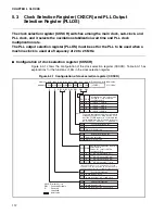
5.3
Clock Selection Register (CKSCR) and PLL Output
Selection Register (PLLOS)
The clock selection register (CKSCR) switches among the main clock, sub-clock, and
PLL clock, and it selects the oscillation stabilization wait time and PLL clock
multiplication rate.
The PLL output selection register (PLLOS) must be set for the PLL to be used when a
machine clock is used at a frequency of 20 to 25 MHz.
■
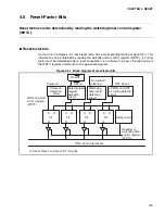
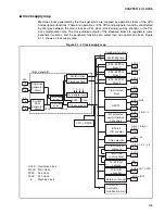
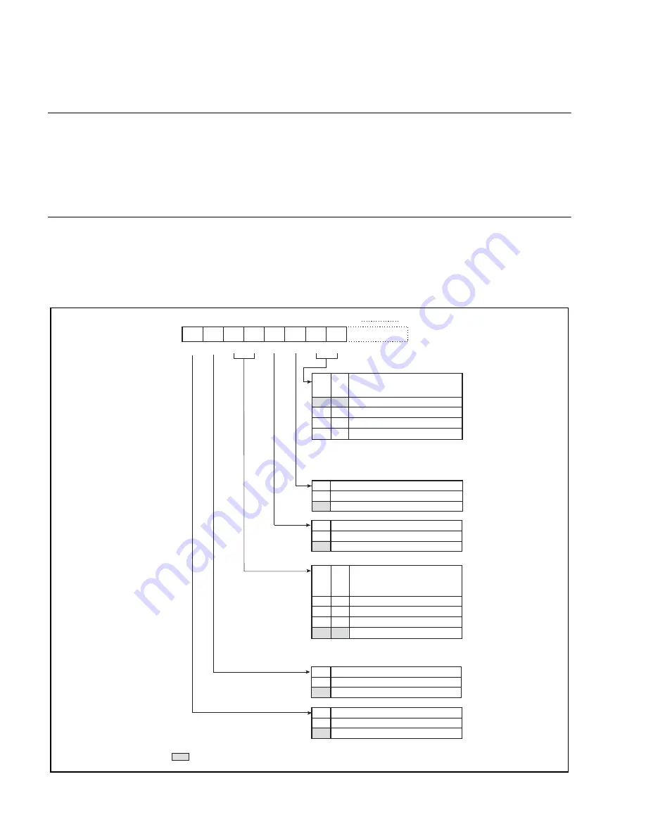
Configuration of clock selection register (CKSCR)
Figure 5.3-1 shows the configuration of the clock selection register (CKSCR). Table 5.3-1 has
explanations for the functions of bits in the clock selection register.
Figure 5.3-1 Configuration of clock selection register (CKSCR)
Address bit15
SCM
R
bit14
MCM
R
bit13
WS1
R/W
bit12
WS0
R/W
bit11
SCS
R/W
bit10
MCS
R/W
bit9
CS1
R/W
bit8 bit7
bit0 Initial value
CS0
(LPMCR)
R/W
0000A1
H
11111100
B
CS1
MCS
SCS
CS0
0
0
0
1
1
0
1
0
1
1
1
×
HCLK ( 4 MHz)
PLL clock selection bit
PLL clock selection
Main clock selection
0
1
Sub clock selection bit
Sub clock selection
Main clock selection
MCM
0
1
PLL clock display bit
In use by PLL clock
In use by main clock or sub clock
SCM
0
1
Sub clock display bit
In use by sub clock
In use by main clock or PLL clock
2
×
HCLK ( 8 MHz)
3
×
HCLK (12 MHz)
4
×
HCLK (16 MHz)
Multiplication rate selection bit
Values in ( ) are for 4 MHz
oscillation clock
WS1 WS0
0
0
0
1
1
0
1
1
2
10
/HCLK (about 256
μ
s)
2
13
/HCLK (about 2.05 ms)
2
15
/HCLK (about 8.19 ms)
2
17
/HCLK (about 32.77 ms)
Oscillation stabilization wait time
selection bits
Values in ( ) are for 4 MHz
oscillation clock
* During a power-on reset, evaluation devices and
FLASH devices become 2
18
/HCLK (about 65.54 ms),
and mask devices become 2
17
/HCLK (about 32.77 ms).
HCLK : Oscillation clock
R/W : Readable/Writable
R
: Read only
-
: Undefined
: Initial value
To ensure the internal circuit operation with
a frequency at 20 to 25 MHz, set the PLL2
bit of the PLLOS register to 1 to double the
above multiply-by rate. However, do not set
the PLL2 bit to 1 when CS1 = 1 and CS0 = 1.
Note:
Summary of Contents for MB90480 Series
Page 2: ......
Page 4: ......
Page 10: ...vi ...
Page 128: ...106 CHAPTER 4 RESET ...
Page 174: ...152 CHAPTER 6 LOW POWER CONSUMPTION MODE ...
Page 198: ...176 CHAPTER 7 MODE SETTING ...
Page 220: ...198 CHAPTER 9 TIMEBASE TIMER ...
Page 238: ...216 CHAPTER 11 WATCH TIMER ...
Page 280: ...258 CHAPTER 12 16 BIT INPUT OUTPUT TIMER ...
Page 406: ...384 CHAPTER 17 8 10 BIT A D CONVERTER ...
Page 478: ...456 CHAPTER 20 CHIP SELECTION FACILITY ...
Page 494: ...472 CHAPTER 21 ADDRESS MATCH DETECTION FUNCTION ...
Page 498: ...476 CHAPTER 22 ROM MIRROR FUNCTION SELECTION MODULE ...
Page 526: ...504 CHAPTER 23 2M 3M BIT FLASH MEMORY ...
Page 536: ...514 CHAPTER 24 EXAMPLES OF MB90F481B MB90F482B MB90F488B MB90F489B SERIAL PROGRAMMING ...
Page 570: ...548 CHAPTER 25 PWC TIMER ONLY MB90485 SERIES ...
Page 688: ......


