
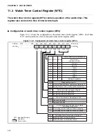


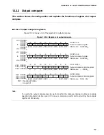

221
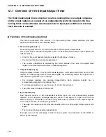
CHAPTER 12 16-BIT INPUT/OUTPUT TIMER
■
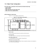
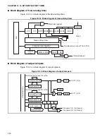
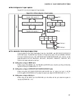
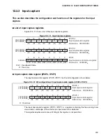
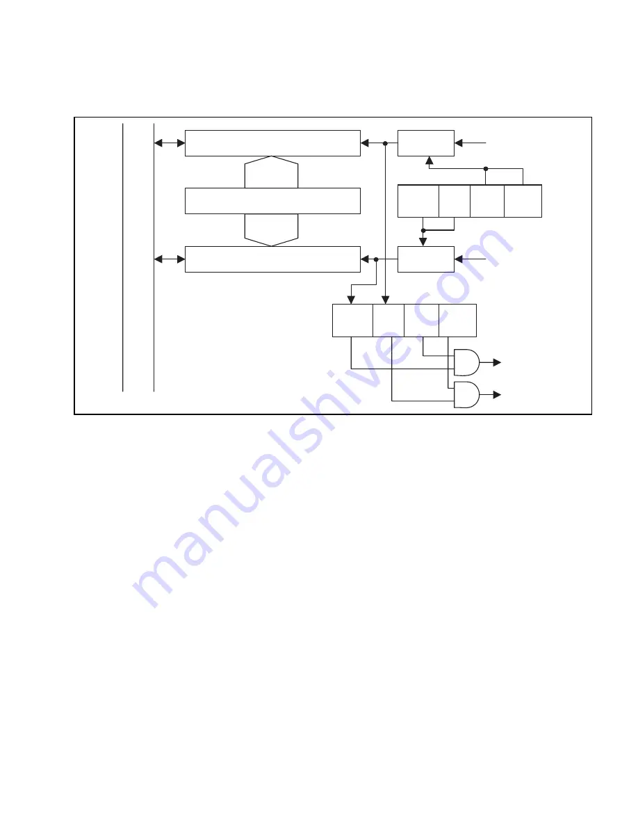
Block diagram of input capture
Figure 12.2-4 is a block diagram of input capture.
Figure 12.2-4 Block diagram of input capture
■
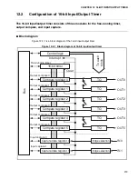
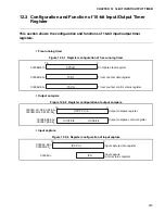
Pin related to 16-bit input/output timer
The pin related to the 16-bit input/output timer has the IN0/IN1 and OUT0/OUT1/OUT2/OUT3/
OUT4/OUT5 pins. The IN0/IN1 pins function as the general-purpose I/O port (P96/IN0, P97/IN1)
and input capture input pin. The OUT0/OUT1/OUT2/OUT3/OUT4/OUT5 pins function as the
general-purpose I/O port (PA0/OUT0, PA1/OUT1, PA2/OUT2, PA3/OUT3, P46/OUT4, P47/
OUT5) and output compare output pin.
●
Setting when using as IN0/IN1 pins
When using as the IN0/IN1 pins, the P96/IN0 and P97/IN1 pins should be set the port direction
register to input port (DDR9 bit15, 14
→
"0").
●
Setting when using as OUT0/OUT1/OUT2/OUT3/OUT4/OUT5 pins
When using the OUT0/OUT1/OUT2/OUT3/OUT4/OUT5 pins as output, be sure to set the
control register (OCS01/23/45) to the output compare pin output (OCS01/23/45 bit10, 11
→
"1").
●
Setting when using as FRCK pin
When using as the FRCK pin, the P93/FRCK pin should be set the port direction register to
input port (DDR9 bit11
→
"0").
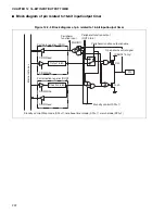
Capture data register 0
Bus
16-bit timer counter value (T15 to T00)
Capture data register 1
Edge detect
Edge detect
EG11 EG10 EG01
EG00
IN1
ICP1
ICP0
ICE1
ICE0
Interrupt
Interrupt
IN0
Summary of Contents for MB90480 Series
Page 2: ......
Page 4: ......
Page 10: ...vi ...
Page 128: ...106 CHAPTER 4 RESET ...
Page 174: ...152 CHAPTER 6 LOW POWER CONSUMPTION MODE ...
Page 198: ...176 CHAPTER 7 MODE SETTING ...
Page 220: ...198 CHAPTER 9 TIMEBASE TIMER ...
Page 238: ...216 CHAPTER 11 WATCH TIMER ...
Page 280: ...258 CHAPTER 12 16 BIT INPUT OUTPUT TIMER ...
Page 406: ...384 CHAPTER 17 8 10 BIT A D CONVERTER ...
Page 478: ...456 CHAPTER 20 CHIP SELECTION FACILITY ...
Page 494: ...472 CHAPTER 21 ADDRESS MATCH DETECTION FUNCTION ...
Page 498: ...476 CHAPTER 22 ROM MIRROR FUNCTION SELECTION MODULE ...
Page 526: ...504 CHAPTER 23 2M 3M BIT FLASH MEMORY ...
Page 536: ...514 CHAPTER 24 EXAMPLES OF MB90F481B MB90F482B MB90F488B MB90F489B SERIAL PROGRAMMING ...
Page 570: ...548 CHAPTER 25 PWC TIMER ONLY MB90485 SERIES ...
Page 688: ......


