


451
CHAPTER 20 CHIP SELECTION FACILITY
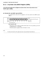
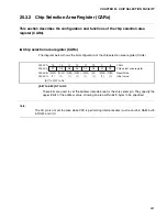
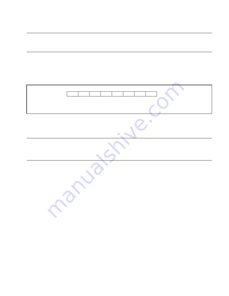
20.3.2 Chip Selection Area Register (CARx)
This section describes the configuration and functions of the chip selection area
register (CARx).
■
Chip selection area register (CARx)
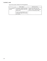
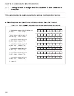
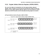
The diagram below shows the bit configuration of the chip selection area register (CARx).
[bit7 to bit0] A7 to A0
These bits are used to set the address decode area for the chip select pin. They specify the
upper 8 bits of the address value, allowing an area within 64 K bytes to be specified.
Note:
The CS pin is not set to active while CPU is performing internal access (such as built-in RAM, built-
in ROM, and I/O).
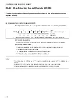
0000C1
H
15
14
13 12 11
10
9
8
CARx
0000C3
H
A7
A6
A5
A4
A3
A2
A1
A0
Chip select area register
0000C5
H
(R/W) (R/W) (R/W) (R/W) (R/W) (W) (R/W) (R/W) Read/Write
0000C7
H
(1) (1) (1) (1) (1) (1) (1) (1) Initial
value
[bit7 to 0]A7 to A0
Summary of Contents for MB90480 Series
Page 2: ......
Page 4: ......
Page 10: ...vi ...
Page 128: ...106 CHAPTER 4 RESET ...
Page 174: ...152 CHAPTER 6 LOW POWER CONSUMPTION MODE ...
Page 198: ...176 CHAPTER 7 MODE SETTING ...
Page 220: ...198 CHAPTER 9 TIMEBASE TIMER ...
Page 238: ...216 CHAPTER 11 WATCH TIMER ...
Page 280: ...258 CHAPTER 12 16 BIT INPUT OUTPUT TIMER ...
Page 406: ...384 CHAPTER 17 8 10 BIT A D CONVERTER ...
Page 478: ...456 CHAPTER 20 CHIP SELECTION FACILITY ...
Page 494: ...472 CHAPTER 21 ADDRESS MATCH DETECTION FUNCTION ...
Page 498: ...476 CHAPTER 22 ROM MIRROR FUNCTION SELECTION MODULE ...
Page 526: ...504 CHAPTER 23 2M 3M BIT FLASH MEMORY ...
Page 536: ...514 CHAPTER 24 EXAMPLES OF MB90F481B MB90F482B MB90F488B MB90F489B SERIAL PROGRAMMING ...
Page 570: ...548 CHAPTER 25 PWC TIMER ONLY MB90485 SERIES ...
Page 688: ......


