

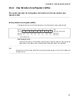


459
CHAPTER 21 ADDRESS MATCH DETECTION FUNCTION
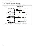
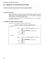
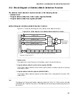
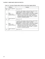
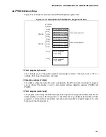
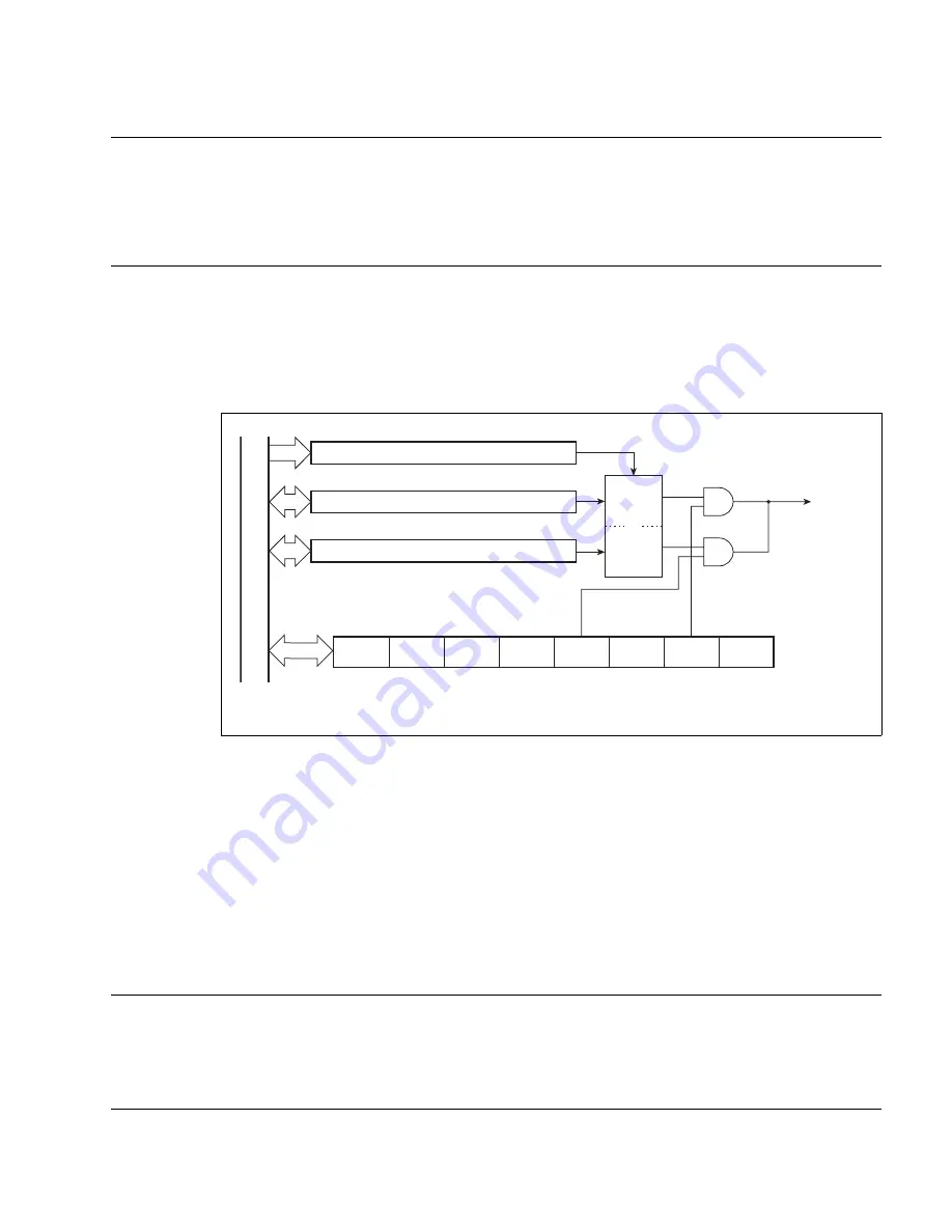
21.2 Block Diagram of Address Match Detection Function
The address match detection module consists of the following blocks:
• Address latch
• Program address detection control status register (PACSR)
• Program address detection registers (RADR)
■
Block Diagram of Address Match Detection Function
Figure 21.2-1 shows the block diagram of the address match detection function.
Figure 21.2-1 Block Diagram of the Address Match Detection Function
❍
Address latch
The address latch stores the value of the address output to the internal data bus.
❍
Program address detection control status register (PACSR)
The program address detection control status register enables or disables output of an interrupt
at an address match.
❍
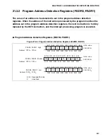
Program address detection registers (PADR0, PADR1)
The program address detection registers set the address that is compared with the value of the
address latch.
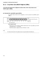
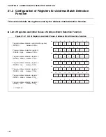
Note:
The addresses of the program address detection register are "1FF0
H
" to "1FF5
H
" and are included
in the RAM area. Therefore, the access to the RAM area should not be performed during the use of
this function.
PADR0 (24
b
it
s
)
Re
s
erved Re
s
erved Re
s
erved ADE1 Re
s
erved ADE0
PAC
S
R
Progr
a
m
a
ddre
ss
detection regi
s
ter 0
Progr
a
m
a
ddre
ss
detection control
s
t
a
t
us
regi
s
ter (PAC
S
R)
Progr
a
m
a
ddre
ss
detection regi
s
ter 1
Addre
ss
l
a
tch
PADR1 (24
b
it
s
)
INT9 in
s
tr
u
ction
(INT9 interr
u
pt
gener
a
tion)
Re
s
erved
Re
s
erved
Inter
n
a
l d
a
t
a
bu
s
Re
s
erved: Alw
a
y
s
s
et to "0"
Comp
a
r
a
tor
Summary of Contents for MB90480 Series
Page 2: ......
Page 4: ......
Page 10: ...vi ...
Page 128: ...106 CHAPTER 4 RESET ...
Page 174: ...152 CHAPTER 6 LOW POWER CONSUMPTION MODE ...
Page 198: ...176 CHAPTER 7 MODE SETTING ...
Page 220: ...198 CHAPTER 9 TIMEBASE TIMER ...
Page 238: ...216 CHAPTER 11 WATCH TIMER ...
Page 280: ...258 CHAPTER 12 16 BIT INPUT OUTPUT TIMER ...
Page 406: ...384 CHAPTER 17 8 10 BIT A D CONVERTER ...
Page 478: ...456 CHAPTER 20 CHIP SELECTION FACILITY ...
Page 494: ...472 CHAPTER 21 ADDRESS MATCH DETECTION FUNCTION ...
Page 498: ...476 CHAPTER 22 ROM MIRROR FUNCTION SELECTION MODULE ...
Page 526: ...504 CHAPTER 23 2M 3M BIT FLASH MEMORY ...
Page 536: ...514 CHAPTER 24 EXAMPLES OF MB90F481B MB90F482B MB90F488B MB90F489B SERIAL PROGRAMMING ...
Page 570: ...548 CHAPTER 25 PWC TIMER ONLY MB90485 SERIES ...
Page 688: ......


