


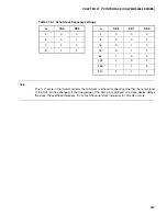
554
CHAPTER 26
μ
PG TIMER (ONLY MB90485 SERIES)
26.3 Timing Chart of
μ
PG Timer
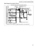
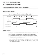
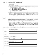
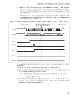
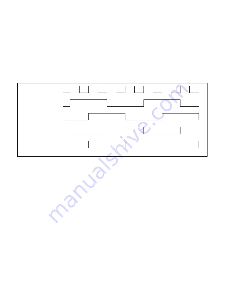
This section shows a timing chart and timing for the
μ
PG timer.
■
Timing chart of
μ
PG timer
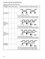
Figure 26.3-1 shows the timing chart of input and output signals for the
μ
PG timer.
Figure 26.3-1 Timing chart of input/output signals for the
μ
PG timer
■
Notes on timing
•
Figure 26.3-1 shows the output waveform against the input waveform. The duty ratio is fixed
at 50%.
•
In sync with the first rising pulse after start, the output starts from the 2nd rising pulse.
•
Two outputs for one input waveform are only issued using inversion control via the program.
•
For the input pulse (waveform at the EXTC pin), use an interval 10 times larger than one
pulse of the internal clock (machine clock).
•
To write "11
B
" for the PE0 and PE1 of the
μ
PG control/status register (allow output for all
pins), keep the value at the input pin (EXTC) constant. Otherwise, if a pulse is input to the
input pin (EXTC) when pin output is allowed, the width of the first output pulse may become
shorter than that of the input pulse.
Input waveform
Output MT00
Output MT01
Inverted output MT00
Inverted output MT01
Summary of Contents for MB90480 Series
Page 2: ......
Page 4: ......
Page 10: ...vi ...
Page 128: ...106 CHAPTER 4 RESET ...
Page 174: ...152 CHAPTER 6 LOW POWER CONSUMPTION MODE ...
Page 198: ...176 CHAPTER 7 MODE SETTING ...
Page 220: ...198 CHAPTER 9 TIMEBASE TIMER ...
Page 238: ...216 CHAPTER 11 WATCH TIMER ...
Page 280: ...258 CHAPTER 12 16 BIT INPUT OUTPUT TIMER ...
Page 406: ...384 CHAPTER 17 8 10 BIT A D CONVERTER ...
Page 478: ...456 CHAPTER 20 CHIP SELECTION FACILITY ...
Page 494: ...472 CHAPTER 21 ADDRESS MATCH DETECTION FUNCTION ...
Page 498: ...476 CHAPTER 22 ROM MIRROR FUNCTION SELECTION MODULE ...
Page 526: ...504 CHAPTER 23 2M 3M BIT FLASH MEMORY ...
Page 536: ...514 CHAPTER 24 EXAMPLES OF MB90F481B MB90F482B MB90F488B MB90F489B SERIAL PROGRAMMING ...
Page 570: ...548 CHAPTER 25 PWC TIMER ONLY MB90485 SERIES ...
Page 688: ......


