


579
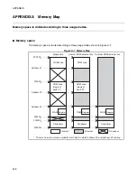
APPENDIX A Memory Map
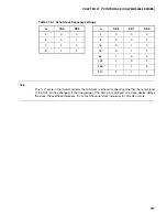
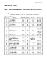
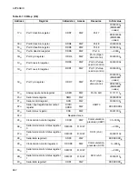
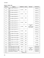
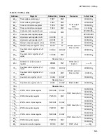
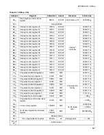
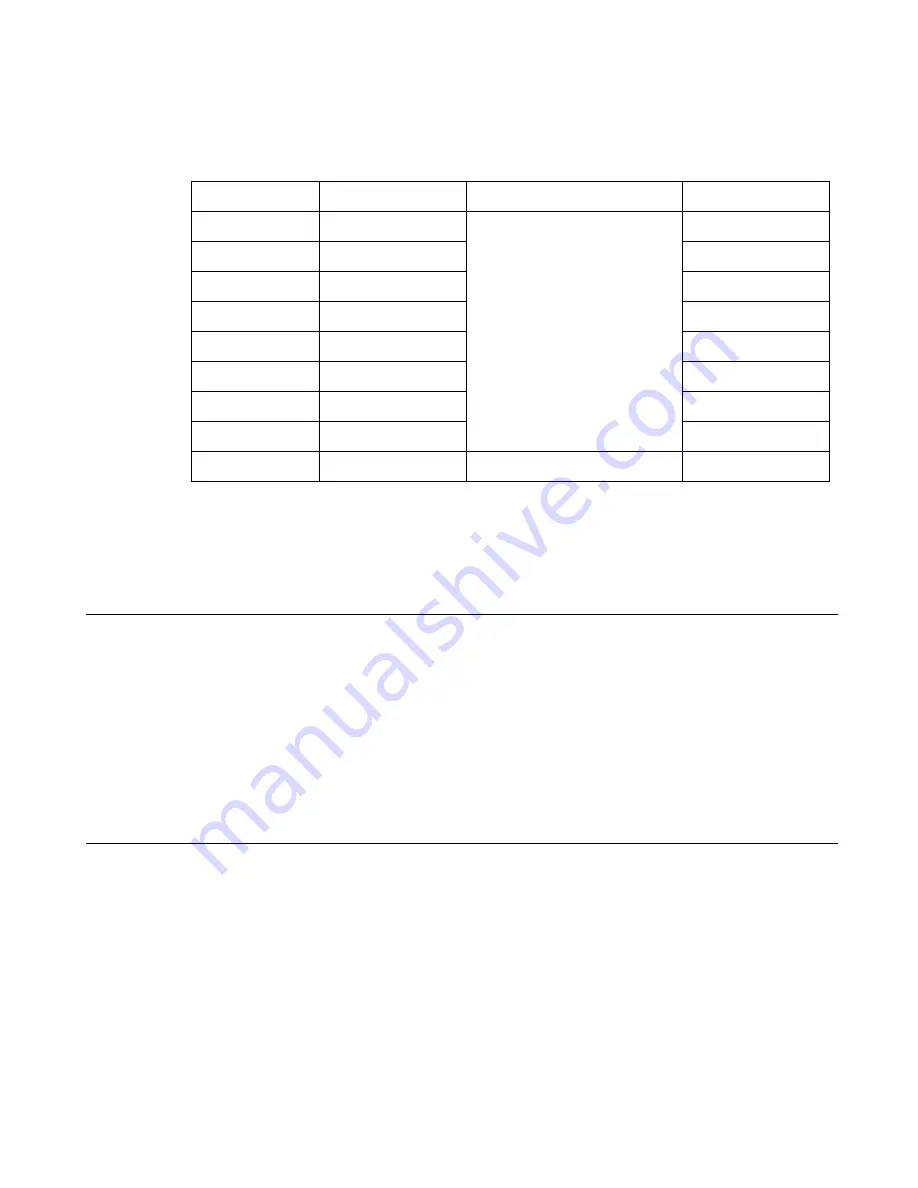
Table A-1 shows the relationship among address #1, address #2, and address #3 for each
product type.
Note:
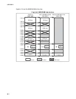
In MB90F481B, the ROM contents of bank FF (between FC0000
H
and FC7FFF
H
or between
FE0000
H
and FE7FFF
H
) can be viewed as an image in the upper part of bank 00, allowing the C
compiler's small model to be more efficiently utilized. Because the lower 16 bits are identical, pointer
declarations do not require the "far" specification to refer the table in ROM. For example, an access
to 00C000
H
will actually be performed as access to the ROM contents at FFC000
H
. However,
because the ROM area in bank FF exceeds 48 KB if the MS bit of the ROMM register is set to "0",
not all of the areas can be viewed via their image in bank 00. For this reason, an image of the area
from FF4000
H
to FFFFFF
H
can be seen in bank 00, while an image of the area from FF0000
H
to
FF3FFF
H
can only be viewed via bank FF.
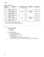
Table A-1 Relationship among address #1, address #2, and address #3 by product type
Type
Address #1
Address #2
Address #3
MB90F481B
FC0000
H
The MS bit of the ROMM
register can be used to select
004000
H
or 008000
H
.
001100
H
MB90F482B
FC0000
H
001900
H
MB90487B
FD0000
H
002900
H
MB90488B
FC0000
H
002900
H
MB90F488B
FC0000
H
002900
H
MB90V480B
(FC0000
H
)
004000
H
MB90V485B
(FC0000
H
)
004000
H
MB90483B
FC0000
H
004000
H
MB90F489B
F90000
H
*
1
0080000
H
fixed
006100
H
*
2
*1: In MB90F489B model, an access to F8 bank and FC bank is not performed in the single-
chip mode and internal ROM/external bus mode as shown in Figure A-2.
*2: Because built-in RAM area in MB90F489B model is larger than that in MB90V485B
model, the emulation area that exceeds 004000
H
must be set the emulation memory area
at tool side.
Summary of Contents for MB90480 Series
Page 2: ......
Page 4: ......
Page 10: ...vi ...
Page 128: ...106 CHAPTER 4 RESET ...
Page 174: ...152 CHAPTER 6 LOW POWER CONSUMPTION MODE ...
Page 198: ...176 CHAPTER 7 MODE SETTING ...
Page 220: ...198 CHAPTER 9 TIMEBASE TIMER ...
Page 238: ...216 CHAPTER 11 WATCH TIMER ...
Page 280: ...258 CHAPTER 12 16 BIT INPUT OUTPUT TIMER ...
Page 406: ...384 CHAPTER 17 8 10 BIT A D CONVERTER ...
Page 478: ...456 CHAPTER 20 CHIP SELECTION FACILITY ...
Page 494: ...472 CHAPTER 21 ADDRESS MATCH DETECTION FUNCTION ...
Page 498: ...476 CHAPTER 22 ROM MIRROR FUNCTION SELECTION MODULE ...
Page 526: ...504 CHAPTER 23 2M 3M BIT FLASH MEMORY ...
Page 536: ...514 CHAPTER 24 EXAMPLES OF MB90F481B MB90F482B MB90F488B MB90F489B SERIAL PROGRAMMING ...
Page 570: ...548 CHAPTER 25 PWC TIMER ONLY MB90485 SERIES ...
Page 688: ......


