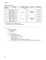

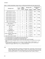


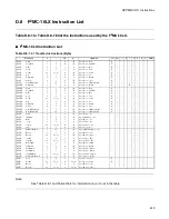
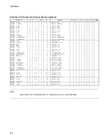
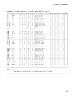
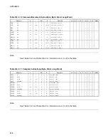
602
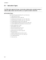
APPENDIX
●
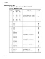
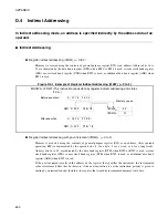
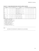
Program counter indirect addressing with offset (@PC + disp16)
Memory is accessed using the address indicated by (instruction a 4 + disp16). The offset is one
word long. Address bits 16 to 23 are specified by the program bank register (PCB). Note that the operand
address of each of the following instructions is not deemed to be (next instruction a disp16):
•
DBNZ eam, rel
•
DWBNZ eam, rel
•
CBNE eam, #imm8, rel
•
CWBNE eam, #imm16, rel
•
MOV eam, #imm8
•
MOVW eam, #imm16
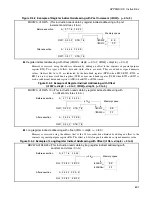
Figure D.4-5 Example of Program Counter Indirect Addressing with Offset (@PC + disp16)
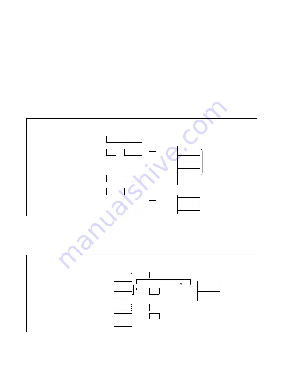
●
Register indirect addressing with base index (@RW0 + RW7, @RW1 + RW7)
Memory is accessed using the address determined by adding RW0 or RW1 to the contents of general-
purpose register RW7. Address bits 16 to 23 are indicated by the data bank register (DTB).
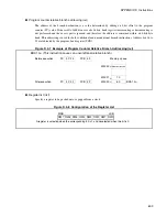
Figure D.4-6 Example of Register Indirect Addressing with Base Index (@RW0 + RW7, @RW1 + RW7)
MOVW A, @PC+20
H
(This instruction reads data by program counter indirect addressing
with an offset and stores it in A.)
Before execution
A
0 7 1 6
2 5 3 4
Memory space
PCB C 5 PC 4 5 5 6
C54556
H
7 3
MOVW
A, @PC+20
H
C54557
H
9 E
C54558
H
2 0
C54559
H
0 0
After execution
A
2 5 3 4
F F E E
+4
C5455A
H
.
.
.
PCB C 5 PC 4 5 5 A
+20
H
C5457A
H
E E
C5457B
H
F F
MOVW A, @RW1+RW7 (This instruction reads data by register indirect addressing with
a base index and stores it in A.)
Before execution
A
0 7 1 6
2 5 3 4
Memory space
RW1 D 3 0 F
+
78D410
H
E E
DTB 7 8
WR7
0 1 0 1
78D411
H
F F
After execution
A
2 5 3 4
F F E E
RW1 D 3 0 F
DTB 7 8
WR7
0 1 0 1
Summary of Contents for MB90480 Series
Page 2: ......
Page 4: ......
Page 10: ...vi ...
Page 128: ...106 CHAPTER 4 RESET ...
Page 174: ...152 CHAPTER 6 LOW POWER CONSUMPTION MODE ...
Page 198: ...176 CHAPTER 7 MODE SETTING ...
Page 220: ...198 CHAPTER 9 TIMEBASE TIMER ...
Page 238: ...216 CHAPTER 11 WATCH TIMER ...
Page 280: ...258 CHAPTER 12 16 BIT INPUT OUTPUT TIMER ...
Page 406: ...384 CHAPTER 17 8 10 BIT A D CONVERTER ...
Page 478: ...456 CHAPTER 20 CHIP SELECTION FACILITY ...
Page 494: ...472 CHAPTER 21 ADDRESS MATCH DETECTION FUNCTION ...
Page 498: ...476 CHAPTER 22 ROM MIRROR FUNCTION SELECTION MODULE ...
Page 526: ...504 CHAPTER 23 2M 3M BIT FLASH MEMORY ...
Page 536: ...514 CHAPTER 24 EXAMPLES OF MB90F481B MB90F482B MB90F488B MB90F489B SERIAL PROGRAMMING ...
Page 570: ...548 CHAPTER 25 PWC TIMER ONLY MB90485 SERIES ...
Page 688: ......


