


605
APPENDIX D Instructions
●
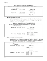
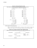
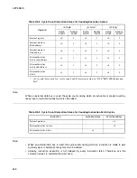
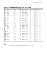
Accumulator indirect branch addressing (@A)
The address of the branch destination is the content (16 bits) of the low-order bytes (AL) of the
accumulator. It indicates the branch destination in the bank address space. Address bits 16 to 23 are
specified by the program bank register (PCB). For the Jump Context (JCTX) instruction, however, address
bits 16 to 23 are specified by the data bank register (DTB). This addressing is used for unconditional
branch instructions.
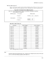
Figure D.4-11 Example of Accumulator Indirect Branch Addressing (@A)
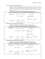
●
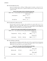
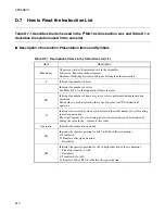
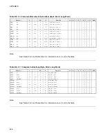
Indirect specification branch addressing (@ear)
The address of the branch destination is the word data at the address indicated by ear.
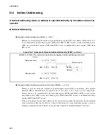
Figure D.4-12 Example of Indirect Specification Branch Addressing (@ear)
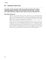
●
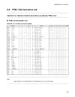
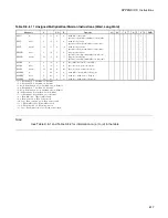
Indirect specification branch addressing (@eam)
The address of the branch destination is the word data at the address indicated by eam.
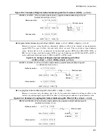
Figure D.4-13 Example of Indirect Specification Branch Addressing (@eam)
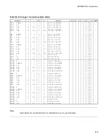
JMP @A (This instruction causes an unconditional branch by accumulator indirect branch addressing.)
Before execution
PC 3 C 2 0
PCB 4 F
Memory space
A
6 6 7 7
3 B 2 0
4F3B20
H
Next instruction
4F3C20
H
6 1
JMP @A
After execution
PC
3 B 2 0
PCB 4 F
A
6 6 7 7
3 B 2 0
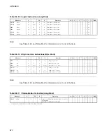
JMP @@RW0 (This instruction causes an unconditional branch by register indirect addressing.)
Before execution
PC 3 C 2 0
PCB 4 F
Memory space
RW0
7 F 4 8
DTB
2 1
217F48
H
2 0
217F49
H
3 B
4F3B20
H
Next instruction
After execution
PC
3 B 2 0
PCB 4 F
4F3C20
H
7 3
JMP @@RW0
4F3C21
H
0 8
RW0
7 F 4 8
DTB
2 1
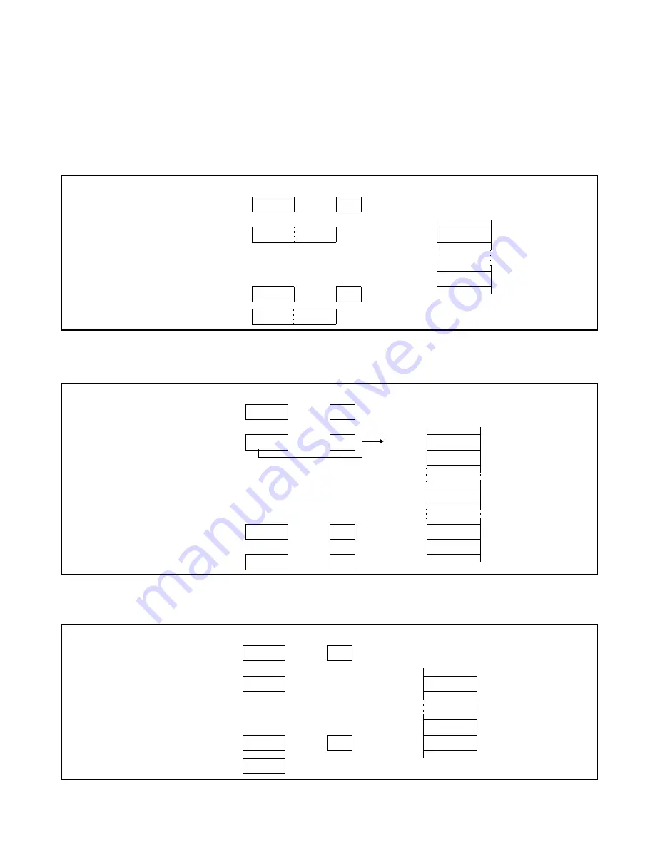
JMP @RW0 (This instruction causes an unconditional branch by register indirect addressing.)
Before execution
PC 3 C 2 0
PCB 4 F
Memory space
RW0
3 B 2 0
4F3B20
H
Next instruction
4F3C20
H
7 3
JMP @RW0
After execution
PC
3 B 2 0
PCB 4 F
4F3C21
H
0 0
RW0
3 B 2 0
Summary of Contents for MB90480 Series
Page 2: ......
Page 4: ......
Page 10: ...vi ...
Page 128: ...106 CHAPTER 4 RESET ...
Page 174: ...152 CHAPTER 6 LOW POWER CONSUMPTION MODE ...
Page 198: ...176 CHAPTER 7 MODE SETTING ...
Page 220: ...198 CHAPTER 9 TIMEBASE TIMER ...
Page 238: ...216 CHAPTER 11 WATCH TIMER ...
Page 280: ...258 CHAPTER 12 16 BIT INPUT OUTPUT TIMER ...
Page 406: ...384 CHAPTER 17 8 10 BIT A D CONVERTER ...
Page 478: ...456 CHAPTER 20 CHIP SELECTION FACILITY ...
Page 494: ...472 CHAPTER 21 ADDRESS MATCH DETECTION FUNCTION ...
Page 498: ...476 CHAPTER 22 ROM MIRROR FUNCTION SELECTION MODULE ...
Page 526: ...504 CHAPTER 23 2M 3M BIT FLASH MEMORY ...
Page 536: ...514 CHAPTER 24 EXAMPLES OF MB90F481B MB90F482B MB90F488B MB90F489B SERIAL PROGRAMMING ...
Page 570: ...548 CHAPTER 25 PWC TIMER ONLY MB90485 SERIES ...
Page 688: ......


