

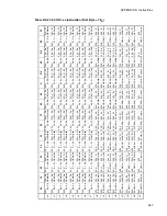


651
Block diagram of pin related to I
2
C interface
Block diagram of pin related to
μ
PG timer
Block diagram of pin related to PWC timer
Block diagram of pin related to UART
Block diagram of PWC timer
................................ 517
Block diagram of the 16-bit reload timer
Block diagram of the 8/16-bit PPG timer
Block diagram of the chip selection facility
Block diagram of the I
2
C interface
.......................... 557
Block diagram of the ROM mirror function selection
module
................................................ 474
Block diagram of timebase timer
............................ 188
Block diagram of watch timer
................................ 211
Block diagram of watchdog timer
........................... 203
......................................... 409
Buffer
Buffer address pointer (BAP)
............................ 74, 84
Bus
Bus error
.......................................................... 575
Bus status register (IBSR)
..................................... 560
Notes on using the bus control register (IBCR)
Bus control
Bus control register (IBCR)
.................................. 562
Bus control signal selection register (EPCR)
Bus mode
Bus mode setting bit (M1,M0)
............................... 157
Bus modes
........................................................ 154
C
CALR
Chip selection active level register (CALR)
CARx
Chip selection area register (CARx)
CCR
Condition code register (CCR)
................................. 33
CCRH
Counter control register (ch0) upper (CCRH0)
Counter control register (ch1) upper (CCRH1)
CCRL
Counter control register (ch0/ch1) lower
(CCRL0/1)
........................................... 269
CDCR
Communication prescaler control register
............................................... 419
Chip
Chip/sector erase operation
................................... 489
Write/chip sector erase operation
............................ 492
Write/chip sector erase operations
.......................... 491
Chip erase
Erasing all data in the flash memory (chip erase)
Chip select
Block diagram of pin related to chip select
facility
................................................ 448
Chip selection
Block diagram of the chip selection facility
Chip selection active level register (CALR)
Chip selection area MASK register (CMRx)
Chip selection area register (CARx)
Chip selection control register (CSCR)
Example of using the chip selection facility
List of registers used for the chip selection
facility
.................................................449
Notes on using the chip selection facility
Overview of the chip selection facility
Pin related to chip selection facility
Circuit type
I/O circuit type
.....................................................18
CKSCR
Configuration of clock selection register
(CKSCR)
.............................................112
Clear
Count clear/gate function
......................................283
Clearing
Clearing the counter
.............................................283
Clearing the timer
................................................537
CLK
Operation in CLK synchronous mode
(operation mode 2)
.................................430
Clock
Block diagram of clock generator
............................110
................................568
Clock source for watchdog timer specifying
function
...............................................215
Clock supply map
................................................109
Clock supplying function
..............................187, 194
Configuration of clock selection register
(CKSCR)
.............................................112
Count clock selection
...........................................533
.............................................292
Oscillation clock frequency and serial clock input
frequency
.............................................508
..............................................108
UART clock selection
..........................................424
Clock mode
..........................................117
Switching the clock mode
.....................................149
......................................................125
CMR
Common register bank prefix (CMR)
CMRx
Chip selection area MASK register (CMRx)
Code
Continuous prefix codes
..........................................42
Command sequence
Command sequence table
......................................486
Common
Common register bank prefix (CMR)
Communication prescaler
Communication prescaler control register
...............................................419
Communication prescaler control register0/1
(SDCR0/SDCR1)
...................................395
Compare
Compare clear register (CPCLR)
............................224
Compare function
Summary of Contents for MB90480 Series
Page 2: ......
Page 4: ......
Page 10: ...vi ...
Page 128: ...106 CHAPTER 4 RESET ...
Page 174: ...152 CHAPTER 6 LOW POWER CONSUMPTION MODE ...
Page 198: ...176 CHAPTER 7 MODE SETTING ...
Page 220: ...198 CHAPTER 9 TIMEBASE TIMER ...
Page 238: ...216 CHAPTER 11 WATCH TIMER ...
Page 280: ...258 CHAPTER 12 16 BIT INPUT OUTPUT TIMER ...
Page 406: ...384 CHAPTER 17 8 10 BIT A D CONVERTER ...
Page 478: ...456 CHAPTER 20 CHIP SELECTION FACILITY ...
Page 494: ...472 CHAPTER 21 ADDRESS MATCH DETECTION FUNCTION ...
Page 498: ...476 CHAPTER 22 ROM MIRROR FUNCTION SELECTION MODULE ...
Page 526: ...504 CHAPTER 23 2M 3M BIT FLASH MEMORY ...
Page 536: ...514 CHAPTER 24 EXAMPLES OF MB90F481B MB90F482B MB90F488B MB90F489B SERIAL PROGRAMMING ...
Page 570: ...548 CHAPTER 25 PWC TIMER ONLY MB90485 SERIES ...
Page 688: ......


