


50
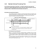
CHAPTER 3 INTERRUPT
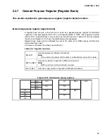
3.3.1
Interrupt Control Register (ICR00 to ICR15)
The interrupt control register (ICR00 to ICR15) corresponds to every peripheral
function that has interrupt functions for controlling processing during interrupt
request generation. This register has different functions between write and read
operations.
■
Interrupt control register (ICR00 to ICR15) function
The interrupt control register (ICR00 to ICR15) consists of bit having the following four functions:
•
Interrupt level setting bit (IL2 to IL0)
•
Extended intelligent I/O service (EI
2
OS) permission bit (ISE3)
•
Extended intelligent I/O service (EI
2
OS) channel selection bits (ICS3 to ICS0)
•
Extended intelligent I/O service (EI
2
OS) status bits (S1, S0)
■
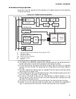
Configuration of interrupt control register (ICR00 to ICR15)
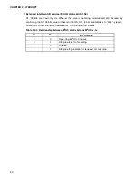
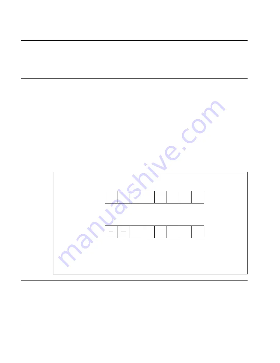
Figure 3.3-1 shows the bit configuration of the interrupt control register (ICR00 to ICR15).
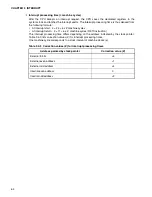
Figure 3.3-1 Bit configuration of interrupt control register (ICR00 to ICR15)
Notes:
• Only when extended intelligent I/O service (EI
2
OS) is started, the ICS3 to ICS0 bits are valid.
Please set "1" to the ISE bit when EI
2
OS is started. Please set "0" to the ISE bit when EI
2
OS is
not started. When EI
2
OS is not started, the setting of the ICS3 to ICS0 bits are unnecessary.
• ICS1, ICS0 bits can be only write. S1, S0 bits can be only read.
Address
0000B0
H
0000BF
H
bit7
bit6
bit5
bit4
bit3
bit2
bit1
bit0
R/W
IL2
IL1
IL0
00000111
B
Initial value
Interrupt control register (ICR)
R/W
R
W
-
R/W
R/W
R/W
W
W
W
W
: Readable/Writable
: Read only
: Write only
: Undefined
Address
0000B0
H
0000BF
H
bit7
bit6
bit5
bit4
bit3
bit2
bit1
bit0
R/W
IL2
IL1
IL0
XX000111
B
Initial value
Interrupt control register (ICR)
R/W
R/W
R/W
-
-
R
R
ICS3 ICS2 ICS1
ISE
ICS0
S1
ISE
S0
to
to
Summary of Contents for MB90480 Series
Page 2: ......
Page 4: ......
Page 10: ...vi ...
Page 128: ...106 CHAPTER 4 RESET ...
Page 174: ...152 CHAPTER 6 LOW POWER CONSUMPTION MODE ...
Page 198: ...176 CHAPTER 7 MODE SETTING ...
Page 220: ...198 CHAPTER 9 TIMEBASE TIMER ...
Page 238: ...216 CHAPTER 11 WATCH TIMER ...
Page 280: ...258 CHAPTER 12 16 BIT INPUT OUTPUT TIMER ...
Page 406: ...384 CHAPTER 17 8 10 BIT A D CONVERTER ...
Page 478: ...456 CHAPTER 20 CHIP SELECTION FACILITY ...
Page 494: ...472 CHAPTER 21 ADDRESS MATCH DETECTION FUNCTION ...
Page 498: ...476 CHAPTER 22 ROM MIRROR FUNCTION SELECTION MODULE ...
Page 526: ...504 CHAPTER 23 2M 3M BIT FLASH MEMORY ...
Page 536: ...514 CHAPTER 24 EXAMPLES OF MB90F481B MB90F482B MB90F488B MB90F489B SERIAL PROGRAMMING ...
Page 570: ...548 CHAPTER 25 PWC TIMER ONLY MB90485 SERIES ...
Page 688: ......


