201
CHAPTER 10 WATCHDOG TIMER
10.2 Watchdog Timer Control Register (WDTC)
The watchdog timer control register (WDTC) is used for the start and clearing of the
watchdog timer and the display of reset causes.
■
Watchdog timer control register (WDTC)
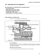
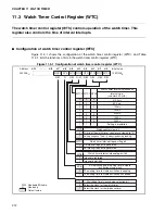
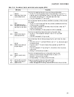
Figure 10.2-1 shows the configuration of the watchdog timer control register (WDTC), and Table
10.2-1 explains the function of each bit in the WDTC register.
Figure 10.2-1 Watchdog timer control register (WDTC)
The interval time is 3.5 to 4.5 times as large as the count clock (output value of the timebase
timer) cycle. See Section "10.4 Watchdog Timer Operation", for details.
Addre
ss
b
it15
b
it7
b
it
8
b
it6
b
it5
b
it4
b
it
3
b
it2
b
it1
b
it0
Initi
a
l v
a
l
u
e
0000A
8
H
XXXXX111
B
(TBTC)
WT1 WT0
WR
S
T
PONR
Re
s
erved
ER
S
T
S
R
S
T WTE WT1
WT0
R
0
0
0
0
0
0
0
0
0
0
0
1
0
1
1
1
1
1
0
1
0
1
1
1
1
R
R
R
W
W
W
WDC
S
&
S
CM
Interv
a
l time
s
election
b
it (
a
t HCLK: 4 MHz;
S
CLK:
3
2 kHz)
Interv
a
l time
N
u
m
b
er of o
s
cill
a
tion
clock cycle
s
Minim
u
m
M
a
xim
u
m
Approxim
a
tely
3
.5
8
m
s
Approxim
a
tely 4.61 m
s
Approxim
a
tely 14.
33
m
s
Approxim
a
tely 1
8
.
3
m
s
Approxim
a
tely 57.2
3
m
s
Approxim
a
tely 7
3
.7
3
m
s
Approxim
a
tely 45
8
.75 m
s
Approxim
a
tely 5
8
9.
8
2 m
s
Approxim
a
tely 0.457
s
Approxim
a
tely 0.576
s
Approxim
a
tely
3
.5
8
4
s
Approxim
a
tely 4.60
8
s
Approxim
a
tely 7.16
8
s
Approxim
a
tely 9.216
s
Approxim
a
tely 14.
33
6
s
Approxim
a
tely 1
8
.4
3
2
s
(2
14
±
2
11
)/HCLK cycle
s
(2
16
±
2
1
3
)/HCLK cycle
s
(2
1
8
±
2
15
)/HCLK cycle
s
(2
21
±
2
1
8
)/HCLK cycle
s
(2
12
±
2
9
)/
S
CLK cycle
s
(2
15
±
2
12
)/
S
CLK cycle
s
(2
16
±
2
1
3
)/
S
CLK cycle
s
(2
17
±
2
14
)/
S
CLK cycle
s
HCLK: O
s
cill
a
tion clock
S
CLK:
Sub
-clock
WTE
W
a
tchdog control
b
it
S
t
a
rt
s
the w
a
tchdog timer
(
a
t fir
s
t write event
a
fter re
s
et)
Cle
a
r
s
the w
a
tchdog timer
(
a
t
s
econd write event
a
fter re
s
et)
No oper
a
tion
Undefined
b
it
Re
a
ding
a
nd writing h
as
no effect on oper
a
tion
Re
s
et c
aus
e
b
it
s
Re
s
et c
aus
e
1 X X X
Power
on
*
1
*
*
W
a
tchdog timer
*
*
1
*
Extern
a
l pin (R
S
T = "L" inp
u
t)
*
*
*
1
R
S
T
b
it (
s
oftw
a
re re
s
et)
PONR WR
S
T ER
S
T
S
R
S
T
R :
Re
a
d only
W :
Write
only
x :
Undefined
- :
Undefined
*
:
The
previo
us
s
t
a
te i
s
held.
:
Def
au
lt v
a
l
u
e
1
Summary of Contents for MB90480 Series
Page 2: ......
Page 4: ......
Page 10: ...vi ...
Page 128: ...106 CHAPTER 4 RESET ...
Page 174: ...152 CHAPTER 6 LOW POWER CONSUMPTION MODE ...
Page 198: ...176 CHAPTER 7 MODE SETTING ...
Page 220: ...198 CHAPTER 9 TIMEBASE TIMER ...
Page 238: ...216 CHAPTER 11 WATCH TIMER ...
Page 280: ...258 CHAPTER 12 16 BIT INPUT OUTPUT TIMER ...
Page 406: ...384 CHAPTER 17 8 10 BIT A D CONVERTER ...
Page 478: ...456 CHAPTER 20 CHIP SELECTION FACILITY ...
Page 494: ...472 CHAPTER 21 ADDRESS MATCH DETECTION FUNCTION ...
Page 498: ...476 CHAPTER 22 ROM MIRROR FUNCTION SELECTION MODULE ...
Page 526: ...504 CHAPTER 23 2M 3M BIT FLASH MEMORY ...
Page 536: ...514 CHAPTER 24 EXAMPLES OF MB90F481B MB90F482B MB90F488B MB90F489B SERIAL PROGRAMMING ...
Page 570: ...548 CHAPTER 25 PWC TIMER ONLY MB90485 SERIES ...
Page 688: ......

