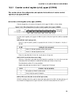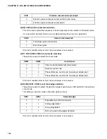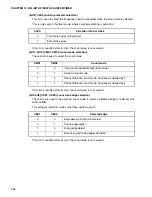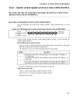
background image

261

CHAPTER 13  8/16-BIT UP/DOWN COUNTER/TIMER

13.2

Configuration of 8/16-bit Up/Down Counter/Timer

The 8-bit up/down counter/timer has two channels and consists of three event input 
pins, one 8-bit up/down count, and one 8-bit reload/compare register per channel. 
Also, one of two 8-bit up/down counter/timer channels can be used as the 16-bit up/
down counter/timer. (When using as the 16-bit up/down counter/timer, the register of 
ch.0 is valid.)

Block diagram of 8/16-bit up/down counter/timer

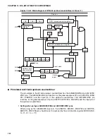
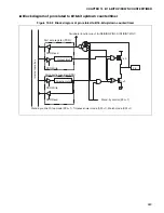
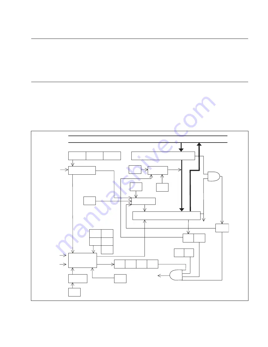
Figure 13.2-1 and Figure 13.2-2 are block diagrams of the 8/16-bit up/down counter/timer.

Figure 13.2-1  Block diagram of 8/16-bit up/down counter/timer (channel 0)

Data bus

CGE1

CGE0

CGSC

8 bits

8 bits

RCR0 (reload/compare register 0)

ZIN0

UDCC

Edge/level 
detected

CTUT

Reload 
control

UCRE

RLDE

Counter clear

UDCR0 (up/down count register 0)

Carry

 CMPF

CMS1 CMS0

CES1 CES0

UDMS

AIN0

BIN0

Up/down count 
clock selection

UDF1 UDF0  CDCF CFIE 

CITE UDIE

Count clock

Interrupt 
output

CSTR

CLKS

Prescaler

UDFF OVFF

Summary of Contents for MB90480 Series

Page 1: ...FUJITSU SEMICONDUCTOR CONTROLLER MANUAL F2 MC 16LX 16 BIT MICROCONTROLLER MB90480 485 Series HARDWARE MANUAL CM44 10121 5E ...

Page 2: ......

Page 3: ... the following support page URL http www fujitsu com global services microelectronics product micom support index html Check Sheet lists the minimal requirement items to be checked to prevent problems beforehand in system development Be sure to refer to the Check Sheet for the latest cautions on development ...

Page 4: ......

Page 5: ...D ROMs and VTRs This manual intended for engineers developing products using the MB90480 485 series explains the MB90480 485 series functions and operations Read this manual first before using the product For details on the instructions refer to the Instruction Manual Note F2 MC is the abbreviation of FUJITSU Flexible Microcontroller Trademark Embedded Algorithm is a registered trademark of Advanc...

Page 6: ...and functions and the operations of the low power consumption mode CHAPTER 7 MODE SETTING This chapter gives an overview of mode setting and explains the mode pins mode data and operation of each mode for mode setting CHAPTER 8 I O PORT This chapter gives an overview of the I O ports and explains the configuration and functions of the registers used by the I O ports CHAPTER 9 TIMEBASE TIMER This c...

Page 7: ...cautions on using the UART and a UART program example CHAPTER 20 CHIP SELECTION FACILITY This chapter gives an overview of the chip selection facility and explains the register configuration and functions and the operation of the chip selection facility CHAPTER 21 ADDRESS MATCH DETECTION FUNCTION This chapter explains the address match detection function and its operation CHAPTER 22 ROM MIRROR FUN...

Page 8: ...ns the register configuration and functions and the operation of the I2 C interface APPENDIX The appendix gives information about the following parts the I O map interrupt vectors and list of instructions It gives detailed information that could not be included in the main text and reference material for programming ...

Page 9: ...ained herein The products described in this document are designed developed and manufactured as contemplated for general use including without limitation ordinary industrial use general office use personal use and household use but are not designed developed and manufactured as contemplated 1 for use accompanying fatal risks or dangers that unless extremely high safety is secured could have a seri...

Page 10: ...vi ...

Page 11: ...40 CHAPTER 3 INTERRUPT 43 3 1 Overview of Interrupt 44 3 2 Interrupt Factor and Interrupt Vector 46 3 3 Interrupt Control Register and Peripheral Function 49 3 3 1 Interrupt Control Register ICR00 to ICR15 50 3 4 Hardware Interrupt 53 3 4 1 Hardware Interrupt Operation 56 3 4 2 Flow of Hardware Interrupt Operation 58 3 4 3 Procedure for Using Hardware Interrupt 59 3 4 4 Multiple Interrupts 61 3 4 ...

Page 12: ...1 5 6 Connecting Oscillator to External Clock 122 CHAPTER 6 LOW POWER CONSUMPTION MODE 123 6 1 Overview of Low Power Consumption Mode 124 6 2 Block Diagram of Low Power Consumption Control Circuit 126 6 3 Low Power Consumption Mode Control Register LPMCR 128 6 4 CPU Intermittent Operation Mode 131 6 5 Standby Mode 132 6 5 1 Sleep Mode 133 6 5 2 Timebase Timer Mode 135 6 5 3 Watch Mode 137 6 5 4 St...

Page 13: ...es on Using Watchdog Timer 207 10 6 Sample Programs of Watchdog Timer 208 CHAPTER 11 WATCH TIMER 209 11 1 Overview of Watch Timer 210 11 2 Watch Timer Configuration 211 11 3 Watch Timer Control Register WTC 212 11 4 Watch Timer Operation 214 CHAPTER 12 16 BIT INPUT OUTPUT TIMER 217 12 1 Overview of 16 bit Input Output Timer 218 12 2 Configuration of 16 bit Input Output Timer 219 12 3 Configuration...

Page 14: ...r TMRLR 301 14 3 Interrupt of 16 Bit Reload Timer 303 14 4 Operations of the 16 Bit Reload Timer 304 14 4 1 State Transitions During Count Operation 305 14 4 2 Operations of Internal Clock Mode Reload Mode 306 14 4 3 Internal Clock Mode One Shot Mode 308 14 4 4 Event Count Mode 310 14 5 Program Example of 16 Bit Reload Timer 312 CHAPTER 15 8 16 BIT PPG TIMER 317 15 1 Overview of 8 16 Bit PPG Timer...

Page 15: ...tatus Register 0 1 SMCS0 SMCS1 390 18 3 2 Serial Data Register 0 1 SDR0 SDR1 394 18 3 3 Communication Prescaler Control Register0 1 SDCR0 SDCR1 395 18 4 Interrupt of Expanded I O Serial Interface 396 18 5 Operation of Expanded I O Serial Interface 397 18 5 1 Shift Clock Modes 398 18 5 2 Operational States of Serial I O Units 399 18 5 3 Start Stop Timing and Input Output Timing of Shift Operation 4...

Page 16: ...h Detection Function 466 21 5 Program Example of Address Match Detection Function 471 CHAPTER 22 ROM MIRROR FUNCTION SELECTION MODULE 473 22 1 Overview of ROM Mirror Function Selection Module 474 22 2 ROM Mirror Function Selection Register ROMM 475 CHAPTER 23 2M 3M BIT FLASH MEMORY 477 23 1 Overview of 2M 3M Bit Flash Memory 478 23 2 Sector Configuration of 2M 3M Bit Flash Memory 479 23 3 Flash me...

Page 17: ...ons of PWC Timer 529 25 5 1 Operations of the Timer Function 530 25 5 2 Operations of the Pulse Width Measurement Function 531 25 5 3 Selection of Count Clock and Operation Mode 533 25 5 4 Start and Stop of Timer Pulse Width Measurement 535 25 5 5 Timer Mode Operation 537 25 5 6 Operation in Pulse Width Measurement Mode 540 25 6 Notes on PWC Timer Usage 546 CHAPTER 26 µPG TIMER ONLY MB90485 SERIES...

Page 18: ...upt Control Register 589 APPENDIX D Instructions 591 D 1 Instruction Types 592 D 2 Addressing 593 D 3 Direct Addressing 595 D 4 Indirect Addressing 600 D 5 Execution Cycle Count 606 D 6 Effective Address Field 609 D 7 How to Read the Instruction List 610 D 8 F2MC 16LX Instruction List 613 D 9 Instruction Map 627 INDEX 649 ...

Page 19: ...no external oscillator or external clock input is stopped Performance of this operation however cannot be guaranteed On this microcontroller if in case the crystal oscillator breaks off or an external reference clock input stops while the PLL clock mode is selected a self oscillator circuit contained in the PLL may continue its operation at its self running frequency However Fujitsu will not guara...

Page 20: ... changed 6 Input cutoff means that operations of input gates located very close to the pins are disabled Output Hi Z means that the pin drive transistors are disabled and the pins are set to the high impedance state 5 In the state of Input cutoff input A is masked and L level is transmitted internally Output Hi Z means that the pin drive transistors are disabled and the pins are set to the high im...

Page 21: ...ial Interface is added 404 to 406 18 6 Program Example of Expanded I O Serial Interface is added 413 bit5 bit4 bit3 CS2 CS1 CS0 Clock Select is changed The use of the clock division ratio 1 1 CS2 to CS0 000B during synchronous transfer is prohibited Please do not use the following settings when dedicated baud rate generator is used at synchronous transfer 1 CS2 to CS0 000B 2 CS2 to CS0 001B DIV3 t...

Page 22: ... enters the erase suspend mode after 15 μs have elapsed or earlier If a erase suspend command is entered during a sector erase operation after the sector erase wait time the system enters the erase suspend mode after 20 μs have elapsed or earlier Please execute the sector erase stop command after sector erase command or sector erase resume command issuing and 20 μs or more 503 Table 23 7 1 Flash S...

Page 23: ... overview of MB90480 485 series including its basic features and basic specifications 1 1 Features of MB90480 485 Series 1 2 Block Diagram of MB90480 485 Series 1 3 Package Dimensions 1 4 Pin Assignment 1 5 Pin Functions 1 6 I O Circuit Type 1 7 Handling the Device ...

Page 24: ...odes 23 types Improved high precision operation using a 32 bit accumulator Signed multiply and divide operations extensive RETI instruction Instruction system supporting multitasking in high level languages such as C Use of a system stack pointer Symmetry of instruction sets and barrel shift instructions Nonmultiplex bus and multiplex bus support Improved execution speed 4 byte queue Improved inte...

Page 25: ...stem clock generator Power saving mode stop mode sleep mode CPU intermittent operation mode watch mode timebase timer mode Package QFP100 LQFP100 CMOS technology 3V single power supply On only MB90485 series some port can be operated on 5V power supply I2C interface 1 channel only for MB90485 series Only MB90487B has built in I2 C interface and its pins P77 P76 are N ch open drain pins not P ch 16...

Page 26: ...90487B MB90F488B MB90488B MB90F489B MB90483B Product configura tion EVA function Mask ROM product Flash memory product Mask ROM product Flash memory product Mask ROM product ROM capacity 192K bytes 256K bytes 256K bytes 384K bytes 256K bytes RAM capacity 16K bytes 10K bytes 10K bytes 10K bytes 24K bytes 16K bytes Description f 25MHz 3 V 5 V power supply 1 Built in PWC μPG I2 C 2 f 25MHz 3 V 5 V po...

Page 27: ...pace are shown in memory map in appendix Power supply consumption Differences among power supply consumption refer to ELECTRICAL CHARACTERISTICS in datasheet Table 1 1 3 MB90480 485 series package and correspondence of product MB90487B 488B MB90483B MB90F481B F482B MB90F488B F489B MB90V480B MB90V485B FPT 100P M06 FPT 100P M05 PGA 299C Usable No usable Product Package ...

Page 28: ...DA EXTC MT00 MT01 PWC0 PWC1 PWC2 Clock control circuit CPU F2MC16LX core Interrupt controller 8 16 bit PPG 8 16 bit up down counter μPG Chip select Input output timer 16 bit input capture 2 channels 16 bit output compare 2 channels 16 bit reload timer I2C interface External interrupt UART I O extended serial interface 2 channels A D converter 10 bit PWC 3 channels I O port to to to to to to to to ...

Page 29: ...ce P LFQFP100 14 14 0 50 100 pin plastic LQFP FPT 100P M05 FPT 100P M05 C 2003 FUJITSU LIMITED F100007S c 4 6 14 00 0 10 551 004 SQ 16 00 0 20 630 008 SQ 1 25 26 51 76 50 75 100 0 50 020 0 20 0 05 008 002 M 0 08 003 0 145 0 055 0057 0022 0 08 003 A INDEX 059 004 008 0 10 0 20 1 50 Mounting height 0 8 0 50 0 20 020 008 0 60 0 15 024 006 0 25 010 0 10 0 10 004 004 Details of A part Stand off Dimensi...

Page 30: ...6 FPT 100P M06 C 2002 FUJITSU LIMITED F100008S c 5 5 1 30 31 50 51 80 81 100 20 00 0 20 787 008 23 90 0 40 941 016 14 00 0 20 551 008 17 90 0 40 705 016 INDEX 0 65 026 0 32 0 05 013 002 M 0 13 005 A 0 17 0 06 007 002 0 10 004 Details of A part 035 006 0 88 0 15 031 008 0 80 0 20 0 25 010 3 00 0 35 0 20 014 008 118 Mounting height 0 25 0 20 010 008 Stand off 0 8 Dimensions in mm inches Note The val...

Page 31: ...gram for the QFP 100 type Figure 1 4 1 Pin assignment diagram of MB90480 485 series QFP 100 FPT 100P M06 MB90480 series only I2C pin P77 and P76 are N ch open drain pin without P ch However MB90V485B uses the N ch open drain pin with P ch P20 to P27 P30 to P37 P40 to P47 and P70 to P77 also used as 3 V 5 V I F pin As for MB90V485B input pins PWC0 PWC1 PWC2 EXTC SCL and SDA pins for PWC μPG I2C bec...

Page 32: ...ent diagram of MB90480 485 series LQFP 100 FPT 100P M05 MB90480 series only I2C pin P77 and P76 are N ch open drain pin without P ch However MB90V485B uses the N ch open drain pin with P ch P20 to P27 P30 to P37 P40 to P47 and P70 to P77 also used as 3 V 5 V I F pin As for MB90V485B input pins PWC0 PWC1 PWC2 EXTC SCL and SDA pins for PWC μPG I2C become CMOS input ...

Page 33: ...put register settings RDR0 a pull up resistor can be set to the enabled state RD00 RD07 1 disabled for the output setting AD00 to AD07 Functions as the lower input output pin of an external address and data bus in the multiplex mode D00 to D07 Functions as the lower output pin of an external data bus in the non multiplex mode 91 to 98 93 to 100 P10 to P17 C CMOS General purpose input output port W...

Page 34: ...utput control register HACR is set to 0 A20 to A23 Functions as the upper output pin of an address A20 to A23 in the non multiplex mode if the bit corresponding to external address output control register HACR is set to 0 PPG0 to PPG3 Functions as the PPG timer output pin 7 9 P30 E CMOS H General purpose input output port A00 Functions as an external address pin in the non multi bus mode AIN0 8 16...

Page 35: ...nctions as an external address pin in the non multiplex mode SOT2 Simple serial I O output pin 18 20 P42 G CMOS H General purpose input output port A10 Functions as an external address pin in the non multiplex mode SCK2 Simple serial I O clock input output pin 19 20 21 22 P43 P44 F CMOS MB90480 series General purpose input output port A11 A12 Functions as an external address pin in the non multipl...

Page 36: ...ster is set to 1 WRH Functions as the write strobe output WRH pin of data on the upper side in the external bus mode of a 16 bit bus width Functions as a general purpose input output port if the WRE bit of the EPCR register is set to 0 72 74 P54 D CMOS General purpose input output port Functions as the HRQ pin in the external bus mode if the HDE bit of the EPCR register is set to 1 HRQ Functions a...

Page 37: ...tput port SCK0 Functions as the UART clock input output pin 28 30 P73 G CMOS H General purpose input output port TIN0 Functions as the event input pin of a 16 bit reload timer 29 31 P74 F CMOS General purpose input output port TOT0 Functions as the output pin of a 16 bit reload timer 30 32 P75 F CMOS MB90480 series General purpose input output port P75 G CMOS H MB90485 series General purpose input...

Page 38: ...external clock input pin when a free running timer is used ADTG Functions as the external trigger input pin when an A D converter is used CS3 Chip select 3 60 62 P94 D CMOS General purpose input output port PPG4 Functions as the output pin of the PPG timer 61 63 P95 D CMOS General purpose input output port PPG5 Functions as the output pin of the PPG timer 62 64 P96 E CMOS H General purpose input o...

Page 39: ...y MB90485 series Power supply pin for 3V or 5V 5V power supply pin In case that P20 to P27 P30 to P37 P40 to P47 and P70 to P77 are used as a 5V I F pin On single 3V power supply voltage this pin is connected with VCC and VCC3 and used for 3V power supply 9 40 79 11 42 81 VSS Power supply input GND 1 LQFP FPT 100P M05 2 QFP FPT 100P M06 3 Refer to 1 6 I O Circuit Type about I O circuit type 4 CMOS...

Page 40: ...marizes the I O circuit type of MB90480 485 series pins Table 1 6 1 I O circuit type 1 3 Class Circuit Description A Oscillation feedback resistor X1 X0 about 1 MΩ X1A X0A about 10 MΩ Use of standby control B Hysteresis input with pull up C Use of input pull up resistor control CMOS level input output X1 X1A X0 X0A Standby control signal Hysteresis input Control CMOS ...

Page 41: ...nput CMOS level output F CMOS level input output Use of open drain control G CMOS level output Hysteresis input Use of open drain control Table 1 6 1 I O circuit type 2 3 Class Circuit Description CMOS CMOS CMOS Open drain control signal CMOS Hysteresis input Open drain control signal ...

Page 42: ...tput J Flash product CMOS level input High voltage control provided for Flash test Mask product CMOS Hysteresis input Table 1 6 1 I O circuit type 3 3 Class Circuit Description CMOS Analog input Hysteresis input Digital output Control signal Mode input Dispersion resistor Flash product CMOS Hysteresis input Mask product ...

Page 43: ...y For an unused A D converter connect it so that AVCC AVRH VCC and AVSS VSS Handling a power supply pin VCC VSS If multiple VCC and or VSS are used all power supply pins must be connected with a power supply or ground externally in consideration of device design in order to decrease latch up and unnecessary radiation and to prevent the malfunction of the strobe signal due to a rise of ground level...

Page 44: ... for stabilization the VCC ripple variation P P value in the commercial frequency 50 60 MHz must be 10 of the standard VCC value or lower or the transient variation must be 0 1 V ms in instantaneous variation including power supply switching To use this product as a single system To use this product which is two system products as a single system use it under the conditions of X0A VSS and X1A OPEN...

Page 45: ...plains CPU specifications memory and the functions of registers to provide readers with a better understanding of the MB90480 485 series functions 2 1 Overview of CPU Specifications 2 2 Memory Space 2 3 CPU Registers 2 4 Prefix Codes ...

Page 46: ...ges expanding addressing modes improving multiply and divide operation instructions and enhancing bit processing The followings are features of F2 MC 16LX CPU Minimum instruction execution time 40 0 ns 6 25 MHz oscillation multiplied by 4 25 MHz 3 3 V 0 3 V for internal operation 62 5 ns 4 MHz oscillation multiplied by 4 16 MHz 3 0 V 0 3 V for internal operation PLL clock multiply scheme Maximum m...

Page 47: ...es with appropriate bank registers and lower 16 bit addresses with instructions Linear addressing has two types one uses operands to directly specify 24 bit addresses the other refers to contents of the lower 24 bits in a 32 bit general purpose register as addresses Linear addressing specified with 24 bit operand Figure 2 2 2 shows an example of linear addressing scheme specified with 24 bit opera...

Page 48: ...SB or SSB is called the stack SP space The SP space is accessed if a stack access occurs by saving the push pop instruction or interrupt register The stack space to be accessed is determined by the S flag in the condition code register A 64K bytes bank specified with ADB is called the additional AD space The AD space includes for example the data that cannot be included in the DT space As shown in...

Page 49: ... RW1 RW4 and RW5 A addr16 dir Stack space Addressing mode using PUCHW POPW RW3 and RW7 Additional space Addressing mode using RW2 and RW6 FEH B3H 92H 68H 4BH FFFFFFH FF0000H B3FFFFH 920000H 68FFFFH 680000H 4BFFFFH 4B0000H 000000H Program space Additional space User stack space Data space System stack space PCB Program counter bank register ADB Additional data bank register USB User stack bank regi...

Page 50: ...r addresses Thus the lower 16 bits of a 32 bit data item is transferred first followed by the upper 16 bits If a reset signal is input immediately after writing the lower bit writing the upper bit may fail Access to data of multi byte length Figure 2 2 6 shows an example for accessing data of a multi byte length In this example MOVW A 030FFFFH is executed Figure 2 2 6 Example for accessing data of...

Page 51: ... area Processor status PS 16 bit register indicating system status Program counter PC 16 bit register containing a program address Direct page register DPR 8 bit register indicating a direct page Program counter bank register PCB 8 bit register indicating a PC space Data bank register DTB 8 bit register indicating a DT space User stack bank register USB 8 bit register indicating a user stack space...

Page 52: ...egister RW0 to RW7 16 bit general purpose register RL0 to RL3 32 bit general purpose register Figure 2 3 2 shows the configuration of a general purpose register Figure 2 3 2 Configuration of general purpose register The relationship between upper and lower bytes in a byte register and word register is represented with the following formula RW i 4 RW i 2 1 256 R i 2 i 0 to 3 The relationship of upp...

Page 53: ...rt improvements in processing efficiency During a transfer of a data item with a lower byte length to AL a sign extension or zero extension is added to the data and the data is saved in AL as a 16 bit data item Also data in AL is handled in either word lengths or byte lengths If an arithmetic operation instruction of byte processing is executed in AL the upper 8 bits in AL before the operation is ...

Page 54: ...e stack processing other than interrupt routines Only SSP is used if stack space is not divided In stack processing the address of upper 8 bits is indicated with SSP SSB and USP USB Resetting USP and SSP does not initialize them but each then has an undefined value Figure 2 3 5 shows the relationship between stack operation instructions and the stack pointer where the S flag is set to 0 and 1 Figu...

Page 55: ...R Figure 2 3 7 shows the configuration of the condition code register Figure 2 3 7 Configuration of condition code register I Interrupt permission flag An interrupt other than software interrupt is permitted if the I flag is set to 1 and masked if set to 0 The I flag is cleared if reset S Stack flag If the S flag is set to 0 USP is enabled as the stack operation pointer and if it is set to 1 SSP i...

Page 56: ...mediate value of 8 bits to RP but only the lower 5 bits are actually used Figure 2 3 8 Configuration of register bank pointer RP Interrupt level mask register ILM The interrupt level mask register ILM consists of 3 bits indicating the level of the CPU interrupt mask Only interrupt request of an interrupt level higher than that represented with the 3 bits is accepted The highest level is indicated ...

Page 57: ...M2 ILM1 ILM0 Level value Permitted interrupt level 0 0 0 0 Interrupt prohibited 0 0 1 1 0 only 0 1 0 2 Level value less than 1 0 1 1 3 Level value less than 2 1 0 0 4 Level value less than 3 1 0 1 5 Level value less than 4 1 1 0 6 Level value less than 5 1 1 1 7 Level value less than 6 ...

Page 58: ... to be executed by CPU An upper 8 bit address is indicated with the program count bank register PCB PC contents are updated by condition branch instructions subroutine call instructions interrupts or resets It may also be used as a base pointer for operand access Figure 2 3 10 explains the program counter PC functions Figure 2 3 10 Program counter PC functions PCB PC FEH ABCDH FEABCDH Next instruc...

Page 59: ...dditional data bank register ADB Initial value 00H Each bank register indicates memory banks to which PC DT SP user SP system and AD space are allocated All bank registers has a length of 1 byte They are initialized to 00H by a reset Bank registers other than PCB can only be read PCB can also be read but writing to PCB is not permitted PCB is updated either when the JMPP CALLP RETP RETI or RETF in...

Page 60: ...8 to 15 of an instruction operand in the direct addressing mode DPR has a length of 8 bits and is initialized to 01H by a reset It also allows reading and writing by instructions Figure 2 3 11 illustrates the generation of a physical address in the direct addressing mode Figure 2 3 11 Generating a physical address in direct addressing mode MSB 24 bit physical address LSB DTB register DPR register ...

Page 61: ...igure 2 3 12 shows the relationship among registers Register bank values are not initialized by a reset the same as for RAM spaces but the state before resetting is kept At power on however the values are undefined Figure 2 3 12 Relationship among registers Table 2 3 2 Register functions R0 to R7 Used as operand in different instructions Note R0 is used as the barrel shift counter or normalization...

Page 62: ...k registers specified with an operand regardless of a prefix Stack operation instruction PUSHW POPW SSB or USB is used depending on the S flag regardless of a prefix I O access instruction MOVA A io MOV io A MOVX A io MOVW A io MOVW io A MOV io imm8 MOVW io imm8 MOBV A io bp MOVB io bp A SETB io bp CLRB io bp BBC io bp rel BBS io bp rel WBTC WBTS The I O space of a bank is used regardless of wheth...

Page 63: ...ix affects the next instruction MOV ILM imm8 An instruction operation is normal but a prefix affects the next instruction Flag change suppress prefix NCC To suppress a flag change specify the flag change suppress prefix code NCC By inserting NCC before an instruction the flag change caused by an instruction is suppressed However be careful if you use instructions listed below String instruction MO...

Page 64: ...rted before an interrupt is suppressed the prefix code affects up to the first instruction that appears after any code other than interrupt suppress instructions as shown in Figure 2 4 2 Figure 2 4 2 Interrupt suppress instruction and prefix code Continuous prefix codes If continuous prefix codes conflict the latest ones are valid as shown in Figure 2 4 3 Such conflicting prefix codes mean PCB ADB...

Page 65: ...ector 3 3 Interrupt Control Register and Peripheral Function 3 4 Hardware Interrupt 3 5 Software Interrupt 3 6 Interrupt by μDMAC 3 7 Interrupt by Extended Intelligent I O Service EI2 OS 3 8 Exception Processing Interrupt 3 9 Stack Operation of Interrupt Processing 3 10 Sample Program of Interrupt Processing 3 11 Delay Interrupt Generation Module ...

Page 66: ...cution of a dedicated instruction for software interrupts e g INT instruction Interrupt by μDMAC μDMAC is a function used to automatically transfer data between peripheral functions and memory Previous data transfers by an interrupt processing program is provided in the same way as the direct memory access DMAC When a transfer for data of a specified count is completed an interrupt processing prog...

Page 67: ...Main program Interrupt start and return processing μDMAC μDMAC μDMAC processing Specified count completed End of request from peripheral function Software interrupt and exception processing Saving dedicated registers in the system stack Hardware interrupt acceptance prohibited I 0 Execution of interrupt return A dedicated register is returned from the system stack to the routine that exists before...

Page 68: ...pt and software interrupt share the same area Table 3 2 1 lists the assignment of interrupt numbers and interrupt vectors Reference For interrupt vectors that are not used Fujitsu recommends specifying such vectors for the address for exception processing Table 3 2 1 Interrupt vectors Software interrupt instruction Vector address L Vector address M Vector address H Mode data Interrupt No Hardware ...

Page 69: ...H INT3 14 FFFFC4H INT4 15 FFFFC0H ICR02 0000B2H INT5 16 FFFFBCH INT6 17 FFFFB8H ICR03 0000B3H INT7 18 FFFFB4H PWC1 Only MB90485 series 19 FFFFB0H ICR04 0000B4H PWC2 Only MB90485 series 20 FFFFACH PWC0 Only MB90485 series 1 21 FFFFA8H ICR05 0000B5H PPG0 PPG1 counter borrow 22 FFFFA4H PPG2 PPG3 counter borrow 23 FFFFA0H ICR06 0000B6H PPG4 PPG5 counter borrow 24 FFFF9CH 8 16 bit U D counter timer ch ...

Page 70: ...ries 39 FFFF60H ICR14 0000BEH A D converter 15 40 FFFF5CH FLASH write delete timebase timer watch timer 1 41 FFFF58H ICR15 0000BFH Delay interrupt generation module 42 FFFF54H x The interrupt request flag cannot be cleared by the interrupt clear signal The interrupt request flag is cleared The interrupt request flag is cleared The stop request is provided 1 Caution The FLASH write erase timebase t...

Page 71: ...5 0000B3H Interrupt control register 03 ICR03 INT6 7 0000B4H Interrupt control register 04 ICR04 PWC1 2 Only MB90485 series 0000B5H Interrupt control register 05 ICR05 8 16 bit PPG timer 0 1 PWC0 Only MB90485 series 0000B6H Interrupt control register 06 ICR06 8 16 bit PPG timer 2 3 4 5 0000B7H Interrupt control register 07 ICR07 8 16UD counter 0 1 input capture 0 0000B8H Interrupt control register...

Page 72: ...register ICR00 to ICR15 Figure 3 3 1 shows the bit configuration of the interrupt control register ICR00 to ICR15 Figure 3 3 1 Bit configuration of interrupt control register ICR00 to ICR15 Notes Only when extended intelligent I O service EI2 OS is started the ICS3 to ICS0 bits are valid Please set 1 to the ISE bit when EI2 OS is started Please set 0 to the ISE bit when EI2 OS is not started When ...

Page 73: ... intelligent I O service EI2 OS channel selection bit ICS3 to ICS0 The ICS3 to ICS0 bits are write only bits and specify the channel of EI2 OS descriptor address is determined depending on the value set to the ICS3 to ICS0 bits The ICS3 to ICS0 bits are initialized to 0000B by reset Table 3 3 3 shows the relation between EI2 OS channel selection bit and the descriptor address Table 3 3 2 Relations...

Page 74: ...nfirming the S1 S0 bits value at the end of EI2 OS S1 S0 bits are initializes to 00B by reset Table 3 3 4 shows the relation between S1 S0 bit and EI2 OS status Table 3 3 4 Relationship between EI2OS status bit and EI2OS state S1 S0 EI2 OS state 0 0 Operating EI2 OS or inactive 0 1 Stop due to end of counting 1 0 Unused 1 1 Stop due to generation of request from resource ...

Page 75: ...are automatically saved to the system stack and the interrupt level currently requested is stored in the interrupt level mask register ILM In this event control then branches to the corresponding interrupt vector Multiple interrupts Multiple hardware interrupts can start at one time μDMAC μDMAC is an automatic transfer function between memory and I O and if the transfer is completed a hardware int...

Page 76: ...al function control registers and data register Figure 3 4 1 shows hardware interrupt operations during writing to the peripheral function control register area Figure 3 4 1 Hardware interrupt requests during writing to peripheral function control register area Table 3 4 1 Hardware interrupt mechanism Hardware interrupt mechanism Function Peripheral function Interrupt enable bit interrupt request ...

Page 77: ...xecuted until execution of a subsequent instruction is completed In this case the subsequent instruction is other than the instructions mentioned above A hardware interrupt is suppressed during execution of software interrupt When a software interrupt starts other interrupt requests are not accepted so that the I flag is cleared to 0 Table 3 4 2 Hardware interrupt suppress instruction Prefix code ...

Page 78: ...with the lower interrupt number has a priority CPU operation acceptance of interrupt requests and interrupt processing CPU compares the levels ICR IL2 to IL0 of received interrupts with the interrupt level mask register ILM If IL ILM and the interrupt is permitted I 1 in PC CCR the interrupt processing microcode starts and interrupt processing is executed after the instruction currently being exec...

Page 79: ...her than the current interrupt processing level the I flag of the condition code register CCR is checked 6 As a result of the check in step 5 if the I flag indicates an interrupt enable I 1 the interrupt operation waits until the instruction currently being executed is completed and then sets ILM to the requested level IL 7 The contents of the resisters are saved and branched to the interrupt proc...

Page 80: ...C updated Main program Interrupt start and return processing μDMAC μDMAC processing Has the specified number of times been completed Or did a peripheral function issue a complete request Software interrupt and exception processing Saving dedicated registers in the system stack I 0 Hardware interrupt prohibited Execution of interrupt return Return of dedicated registers from system stack and then i...

Page 81: ...he operation start state and the interrupt enable bit is set to permit 5 The interrupt level mask register ILM and interrupt enable flag I are set to interrupt acceptable 6 A hardware interrupt request is generated by generation of a peripheral function interrupt 8 9 10 7 6 5 4 3 2 1 Start Initial setup of peripheral functions Setup of the system stack area Setup of ICR in the interrupt controller...

Page 82: ...errupt processing program 8 The interrupt processing program processes peripheral functions because of interrupt generation 9 The interrupt request from peripheral function is canceled 10 The interrupt return instruction is executed and the program is restored to what it was before branching ...

Page 83: ...pleted unless ILM is changed by the I flag In the interrupt processing routine if the I flag in the condition code register CCR is set to interrupt prohibited I in CCR set to 0 or the interrupt level mask register ILM is set to interrupt prohibited ILM set to 000 the starting of multiple interrupts within the interrupt can be temporarily prohibited Note μDMAC cannot be started in duplicate All oth...

Page 84: ...IL0 in ICR In this example if an interrupt request of level 1 or 0 is generated the interrupt with higher priority is executed first End of interrupt processing If interrupt processing is completed and a return instruction RETI is then executed the values of the dedicated registers A DPR ADB DTB PCB PC PS saved in the stack are returned and the values of the interrupt level mask register ILM are s...

Page 85: ...a time period starting after an interrupt request is generated until the instruction currently being executed is completed Sampling is performed in the last cycle of each instruction to determine whether an interrupt request is generated or not Thus during execution of each instruction the CPU is unable to recognize an interrupt request resulting in a waiting time The interrupt request sample wait...

Page 86: ...t interrupt return θ 11 6 x Z machine cycles RETI instruction The interrupt processing time differs depending on the address indicated by the stack pointer Table 3 4 3 lists correction values Z for interrupt processing times One machine cycle corresponds to a clock interval of machine clocks φ Table 3 4 3 Correction values Z for interrupt processing times Address pointed by stack pointer Correctio...

Page 87: ...tion the I flag in the condition code register CCR is set to 0 to mask hardware interrupts To permit a hardware interrupt during software interrupt processing set the I flag to 1 in the software interrupt processing routine Software interrupt operation If the CPU obtains the INT instruction and execute it a microcode for software interrupt processing starts This microcode is used to save the regis...

Page 88: ...icated registers The branch processing is then executed 3 The RETI instruction is executed in user s interrupt processing routine to end interrupt processing Notes on software interrupts If the program counter bank register PCB is set to FFH the CALLV instruction vector area is duplicated with the table for INT vct8 instructions When creating software make sure that the CALLV instruction and INT v...

Page 89: ...eral resource I O DMA transfers are controlled with the a μDMAC enable register b μDMAC stop status register c μDMAC status register and e descriptor assigned to a range of 000100H to 00017FH in RAM STOP requests are issued as a means to stop DMA transfers from a resource After the end of the DMA transfer a flag is set to the bit corresponding to the transfer end channel of the DMA status register...

Page 90: ...rrupt controller An interrupt request from a resource is not used as a DMA start request 1 An interrupt request output from a resource is used as a DMA start request Cleared to 0 when the DMA transfer byte count reaches 0 0000A4H R W 7 6 5 4 3 2 1 0 STP7 R W STP6 STP5 STP4 STP3 STP2 STP1 STP0 DSSR R W R W R W R W R W R W Initial value 00000000B bit R W Readable Writable STPx bit Function 0 Initial...

Page 91: ...er between I O and memory starts 5 For no transfer end The interrupt request of a resource is cleared For transfer end After the DMA transfer ends the μDMAC status register is set to the transfer end flag thereby causing output of an interrupt request to the interrupt controller Figure 3 6 1 μDMAC operations DEx bit Function 0 Initial value No DMA transfer has ended 1 If the DMA transfer ends an i...

Page 92: ...gure 3 6 2 Table 3 6 1 lists the relationship between channel number and DMA descriptor address Figure 3 6 2 Configuration of DMA descriptor MSB LSB H L Descriptor header address Upper 8 bits of data counter DCTH Lower 8 bits of data counter DCTL Upper 8 bits of I O register address pointer IOAH Lower 8 bits of I O register address pointer IOAL DMA control register DMACS Upper 8 bits of buffer add...

Page 93: ... PPG3 counter borrow EN4 4 000120H PPG4 PPG5 counter borrow EN5 5 000128H Input capture channel 0 load EN6 6 000130H Input capture channel 1 load EN7 7 000138H UART receive completed EN8 8 000140H Output compare channel 0 match EN9 9 000148H Output compare channel 1 match EN10 10 000150H Output compare channel 2 match EN11 11 000158H UART transmit completed EN12 12 000160H 16 bit FRT 16 bit reload...

Page 94: ... pointer IOA The I O register address pointer IOA is a register with a length of 16 bits and it indicates the lower address A15 to A0 of the I O register providing a buffer for data transfers All of the upper addresses A23 to A16 are set to 0 Any I O in a range of 000000H to 00FFFFH can be specified with the address Figure 3 6 4 shows the configuration of the I O register address pointer IOA Figur...

Page 95: ... a request from a peripheral function Operation is ended by a request from a peripheral function Data transfer direction specify bit BAP update fixed selection bit Transfer data length setting bit Byte Word IOA update fixed selection bit Always set these bits to 0 Reserve bit I O register address pointer buffer address pointer Buffer address pointer I O register address pointer The buffer address ...

Page 96: ...rol status register DMACS is set to update provided BAP changes at the lower 16 bits BAPM and BAPL but the upper 8 bits BAPH do not change Figure 3 6 6 shows the configuration of BAP Figure 3 6 6 Configuration of buffer address pointer BAP Notes The I O register address pointer IOA can be used to specify an area ranging from 000000H to 00FFFFH The buffer address pointer BAP can be used to specify ...

Page 97: ...system stack area Initial setup of peripheral function Setup of interrupt control register ICR Initial setup of μDMAC controller Execution of user program Start DMA transfer BF 0 DBAP DIOA NO NO NO NO NO NO NO NO NO NO NO NO NO YES YES YES YES YES YES YES YES YES YES YES YES YES ENx 1 of ch concerned STOP request and SE 1 BW 1 BYTEL 0 BAP BAP 2 STPx 1 ENx 0 DTEx 1 generate interrupt generate other...

Page 98: ...time during a continuation of a data transfer depends on the setting of DMA control status register DMACS as shown in Table 3 6 2 Note In units of machine cycles One machine cycle corresponds to one clock interval of the machine clock φ Correction is required depending on the condition at μDMAC execution as shown in Table 3 6 3 Table 3 6 2 μDMAC execution time Setting of IOA update fixed selection...

Page 99: ...ing time If a transfer is ended with an end request from a peripheral function I O If the μDMAC data transfer ends partway DEx 1 because of an end request by a peripheral function I O the data transfer fails and a hardware interrupt starts The μDMAC processing time in this case is calculated with the following formula Z in the formula indicates a correction value for interrupt processing time see ...

Page 100: ...ource the data transfer source needs not to be set for polling Transferring address increment can be set Increment and no update of I O register address ca be set Interrupt by EI2 OS termination Upon completion of the EI2 OS data transfer s the completion condition branches to the interrupt routine The factor for an EI2 OS completion can be confirmed by checking the EI2 OS status bit ICR S1 S0 by ...

Page 101: ...data is transferred based on the address pointers for the transfer origination and destination 5 The interrupt request flag bit of the peripheral function is cleared after the data transferring completed CPU Resource register ISD Buffer Resource register Interrupt Control Register ICR Interrupt controller Interrupt request by I OA by BAP Count by DCT by ICS Memory Space 3 3 4 2 1 5 ISD I OA BAP IC...

Page 102: ...16 channels Figure 3 7 2 Configuration of EI2 OS Descriptor ISD Data counter upper 8bit DCTH Data counter lower 8bit DCTL I O address pointer upper 8bit IOAH EI2 OS Status register ISCS I O address pointer lower 8bit IOAL Buffer address pointer upper 8bit BAPH Buffer address pointer middle 8bit BAPM Buffer address pointer lower 8bit BAPL ISD Starting Address 000100H 8 ICS MSB LSB H L MSB Highest b...

Page 103: ...d descriptor address Channel Descriptor address 0 000100H 1 000108H 2 000110H 3 000118H 4 000120H 5 000128H 6 000130H 7 000138H 8 000140H 9 000148H 10 000150H 11 000158H 12 000160H 13 000168H 14 000170H 15 000178H The address of ISD indicates the first address of 8 byte ...

Page 104: ... register address pointer IOA I O register address pointer IOA is 16 bit register Specifies the lower order address A15 to A0 for the data transfer The higher order address A23 to A16 is set to 00H The area from 000000H to 00FFFFH can be used when specifying an address Figure 3 7 4 Configuration of I O Register Address Pointer IOA Initial value R W Readable Writable X Undefined DCT R W R W R W R W...

Page 105: ...l bit DIR 0 1 I O register address pointer transfer to Buffer address pointer Buffer address pointer transfer to I O register address pointer Data transfer direction specification bit BF 0 1 Update Buffer address pointer after completion transfer 1 Don t update Buffer address pointer after completion transfer IF 0 1 Update I O register address pointer after completion transfer 2 Don t update I O r...

Page 106: ...tting bit BF is set to 0 the lower 16 bit BAPM BAPL is incremented and the higher 8 bit BAPH is not incremented Figure 3 7 6 Configuration of Buffer Address Pointer BAP References The maximum transfer count that can be set by the data counter DCT is 65 536 64K bytes The area that can be set by the I O address pointer IOA is 000000H to 00FFFFH The area that can be set by the buffer address pointer ...

Page 107: ... is set to IOA data transfer Memory is set to BAP Data is set to BAP data transfer Memory is set to IOA Renewal value depends on BW BAP Update IOA Update Renewal value depends on BW EI2OS End processing Clear Peripheral function interrupt request CPU Operation return DCT decrement Set S1 S0 to 00B Clear ISE to 0 Interruption processing Set S1 S0 to 11B Set S1 S0 to 01B ISD ISCS IF BW BF DIR SE DCT...

Page 108: ...ting Interrupt control register ICR setting Peripheral function operation start setting and Interruption enable bit setting Setting of ILM I inside PS Execution of user program Expansion intelligent I O service resetting channel changing Processing of data in the buffer RETI Data transfer NO YES Interruption request and ISE 1 transition to Interrupt processing ISE S1 S0 EI2OS enable bit ICR EI2OS ...

Page 109: ...s shown in Table 3 7 3 interpolation is necessary for the EI2 OS processing time when the data transfer is continued depending on the EI2OS execution condition Table 3 7 2 Extended intelligent I O service execution time EI2OS termination control bit SE setting Terminates due to termination request from the peripheral Ignores termination request from the peripheral IOA update fixed selection bit IF...

Page 110: ...and a hardware interrupt is activated The EI2 OS processing time is calculated with the following formula Z in the formula indicates the interpolation value for the interrupt handling time Table 3 7 4 Reference One machine cycle corresponds to one clock cycle of the machine clock φ EI2 OS processing time when counting terminates EI2 OS processing time when data is transferred 21 6 Z machine cycle ...

Page 111: ...sing equivalent to the INT 10 software interrupt instruction is executed The following processing is executed before exception processing branches to the interrupt routine The A DPR ADB DTB PCB PC and PS registers are saved to the system stack The I flag of the condition code register CCR is cleared to 0 and hardware interrupts are suppressed The S flag of the condition code register CCR is set to...

Page 112: ... interrupt processing starts Figure 3 9 1 Stack operation at start of interrupt processing Stack operation during return from interrupt processing At the end of interrupt processing if the interrupt return instruction RSTI is executed PS PC PCB DTB ADB DPR and A values are returned from the stack in the reverse order of the start of the interrupt processing The dedicated registers are then restore...

Page 113: ...area user stack area and data area while avoiding duplication with one another System stack and user stack Interrupt processing uses the system stack area Even if the user stack area is being used when an interrupt occurs it is forcibly switched to the system stack Thus the system that primarily uses the user stack area must also correctly prepare the system stack area Use only the system stack un...

Page 114: ...eader bank MOV ILM 07H PS ILM is set to level 7 MOV A STACK_T Setting of system stack MOV SSB A MOVW A STACK_T Setting of stack pointer where MOVW SP A it is set to SSP since S flag 1 MOV DDR1 00000000B P10 INT0 pin is set to input OR CCR 40H I flag in PS CCR is set for interrupt enable MOV I ICR00 00H Interrupt set to level 0 highest MOV I ELVR 00000001B INT0 is set to H level request MOV I EIRR ...

Page 115: ...module delay interrupt factor originate clear register DIRR delayed interrupt request register has the register configuration shown below The delay interrupt factor originate clear register DIRR is a register used to generate clear the delay interrupt factor Writing 1 to the register results in a request to delay an interrupt and writing 0 clears the delay interrupt request Resetting causes the fa...

Page 116: ...t level is higher than that of the ILM bit the hardware interrupt processing micro program starts immediately after the instruction currently being executed is completed As a result the interrupt routine for this interrupt is executed By writing 0 to the relevant DDIR bit within the interrupt processing routine this interrupt factor is cleared and the task is switched The above operation flow is i...

Page 117: ...apter explains reset for the MB90480 485 series 4 1 Overview of Reset 4 2 Reset Factors and Oscillation Stabilization Wait Time 4 3 External Reset Pin 4 4 Resetting 4 5 Reset Factor Bits 4 6 Condition of Pins as Result of Reset ...

Page 118: ...wever oscillation stabilization wait time of MB90F488B F489B becomes 218 215 HCLK about 73 73 ms when the oscillation clock is 4MHz A reset is performed after the end of the oscillation stabilization wait time Watchdog reset A watchdog reset is triggered by a watchdog timer overflow if 0 is not written in the watchdog control bit WTE of the watchdog timer control register WDTC within a preset time...

Page 119: ... requests are also accepted when a bus cycle extension with pin RDY continues for more than 16 machine cycles during external bus access Software reset In a software reset an internal reset is triggered by writing 0 in the internal reset signal bit RST of the low power consumption mode control register LPMCR A software reset does not require the oscillation stabilization wait time Reference Defini...

Page 120: ...1 Reset factors and oscillation stabilization wait time Reset factors Oscillation stabilization wait time The value in parentheses is a period when oscillation clock is 4 MHz Power on reset Evaluation devices FLASH devices 218 HCLK about 65 54 ms Mask devices 217 HCLK about 32 77 ms Watchdog timer None Bits WS1 and WS0 are initialized to 11B External reset via pin RST None Bits WS1 and WS0 are ini...

Page 121: ...y a oscillation stabilization wait time suitable for the oscillator used Refer to Section 5 5 Oscillation Stabilization Wait Time for more information Reset state waiting for stable oscillation A reset during the power on sequence and a reset in response to a reset request in the stop and sub clock modes is performed after the end of the oscillation stabilization wait time created by the timebase ...

Page 122: ...3 1 shows the block diagram of internal reset Figure 4 3 1 Block diagram of internal reset Note To prevent damage to the memory contents by a reset during writing input to pin RST is accepted in a cycle that precludes damage to memory contents A clock is required to initialize internal circuits Input of a clock is required during input of a reset when an external clock is used for operation Pin RS...

Page 123: ...Mode Pins MD2 to MD0 for details of the mode pins Mode fetch After a reset is canceled the CPU transfers the reset vectors and mode data to the applicable registers in the CPU core The reset vectors and mode data are allocated to four bytes namely FFFFDCH to FFFFDFH Upon a reset cancellation the CPU immediately outputs these addresses to a bus and fetches reset vectors and mode data During mode fe...

Page 124: ...when the single chip mode and internal ROM external bus mode are used Mode data Address FFFFDFH The data in the mode register can be modified only by a reset and the mode register settings become effective after a reset Refer to Section 7 3 Mode Data for details on mode data Reset vector Address FFFFDCH to FFFFDEH Write the execution start address after the end of a reset Execution starts from thi...

Page 125: ...eset cancellation run software to process the read value of the WDTC register and branch to an appropriate program Figure 4 5 1 Block diagram of reset factor bits F F RST L S R Q F F S R Q F F S R Q F F S R Q Pin RST No periodic clearing RST bit set Power on Delay circuit F2 MC 16LX Internal bus Power on detection circuit Watchdog timer reset detection circuit S Set R Reset Q Output F F Flip flop ...

Page 126: ...ower on reset bit PONR of the reset factor bits is set to 1 However the reset factor bits other than bit PONR are undefined Therefore if bit PONR is 1 create software so that reset factor bits other than bit PONR are ignored Clearing reset factor bits The reset factor bits is cleared only if the data in the WDTC register is read Bits corresponding to reset factors that have occurred once are not c...

Page 127: ...te and mode data is read from internal ROM Refer to Section 6 7 Pin State in Standby Mode Hold and Reset for the states of pins during a reset Pin states after mode data Is read The states of the pins after mode data is read are determined by mode data M1 M0 If the single chip mode is set M1 M0 00B All I O pins resource pins become set at the high impedance state and mode data is read from the int...

Page 128: ...106 CHAPTER 4 RESET ...

Page 129: ... the MB90480 485 series 5 1 Overview of Clocks 5 2 Block Diagram of Clock Generator 5 3 Clock Selection Register CKSCR and PLL Output Selection Register PLLOS 5 4 Clock Modes 5 5 Oscillation Stabilization Wait Time 5 6 Connecting Oscillator to External Clock ...

Page 130: ...peed oscillation pin or by inputting an external clock Sub clock SCLK This clock operates the watch timer It can also be used as a low speed machine clock This clock is divided by four and created by connecting an oscillator to the low speed oscillation pin or by inputting an external clock Main clock MCLK This is a clock of the oscillation clock divided by two and is used as an input clock to the...

Page 131: ...0 1 BIN0 1 ZIN0 1 TOT0 FRCK IN0 1 CS0 1 2 3 SCK0 SIN0 SCK1 2 SIN1 2 SOT0 SOT1 2 Pin Pin Pin Pin Pin Pin Pin Pin Pin Pin OUT0 1 2 3 4 5 Pin Pin Pin AN0 to AN7 ADTG Pin Pin Pin Sub clock generator circuit Watch timer Watchdog timer Peripheral functions 8 16 bit PPG timer 0 8 16 bit PPG timer 1 8 16 bit PPG timer 2 16 bit reload timer UART0 I O extensive serial interface 2 channels 8 16 bit U D count...

Page 132: ...peration selector Pin high impedance control Internal reset CPU clock CPU clock control circuit Peripheral clock control circuit Intermittent cycle selection Stop and sleep signal Stop signal Peripheral clock Selector for waiting time to stable oscillation Machine clock Cancel waiting time to stable oscillation Clock selector Clock selection register CKSCR Timebase timer To watchdog timer Internal...

Page 133: ... main clock sub clock and four PLL clocks supplied to the CPU clock control circuit and peripheral clock control circuit Clock selection register CKSCR This register changes between the oscillation clock and PLL clocks selects the oscillation stabilization wait time and selects the multiplication rate of the PLL clocks PLL output selection register PLLOS Use this register to specify doubling of th...

Page 134: ...1 HCLK 4 MHz PLL clock selection bit PLL clock selection Main clock selection 0 1 Sub clock selection bit Sub clock selection Main clock selection MCM 0 1 PLL clock display bit In use by PLL clock In use by main clock or sub clock SCM 0 1 Sub clock display bit In use by sub clock In use by main clock or PLL clock 2 HCLK 8 MHz 3 HCLK 12 MHz 4 HCLK 16 MHz Multiplication rate selection bit Values in ...

Page 135: ...Oscillation stabilization wait time selection bits Selects the waiting time for stable oscillation of oscillation clock in a change from the sub clock mode to the main clock mode or from the sub clock mode to the PLL clock mode if the stop mode is canceled Initialized to 11B by all reset factors Note The specified value of the waiting time for stable oscillation must be suitable for the oscillator...

Page 136: ...pt request flag bit TBOF of the timebase timer control register TBTC is also cleared When the main clock is switched to PLL clock mode the oscillation stabilization wait time is fixed at 214 HCLK The oscillation stabilization wait time is about 4 1 ms if the oscillation clock has a frequency of 4 MHz When sub clock mode is switched to PLL clock the oscillation stabilization wait time uses the spec...

Page 137: ...ation of PLL output selection register PLLOS Address Initial value PLL output frequency doubling selection bit Use the multiply by rate set in the CS1 and CS0 bits of the CKSCR register unchanged PLL2 DIV2 0 0 1 1 Double the multiply by rate set in the CS1 and CS0 bits of the CKSCR register PLL input divided selection bit Input the input frequency to PLL Two dividing the input frequency and it inp...

Page 138: ... 1 CS0 bit 0 PLLOS register DIV2 bit 1 PLL2 bit 1 It is possible to set the following during PLL 2 4 multiplication setting and internal clock with 20 MHz fCP 25MHz PLL 2 multiplication CKSCR register CS1 bit 0 CS0 bit 0 PLLOS register DIV2 bit 0 PLL2 bit 1 PLL 4 multiplication CKSCR register CS1 bit 0 CS0 bit 1 PLLOS register DIV2 bit 0 PLL2 bit 1 Please set DIV2 bit of PLLOS register 0 and PLL2 ...

Page 139: ...om the main clock mode to the PLL clock mode Rewriting the MCS bit in the CKSCR register from 1 to 0 in the main clock mode changes the main clock to the PLL clock after the end of the oscillation stabilization wait time of the PLL clock 214 HCLK Change from the PLL clock mode to the main clock mode Rewriting the MCS bit in the CKSCR register from 0 to 1 in the PLL clock mode changes the PLL clock...

Page 140: ...CM and sub clock display bit SCM in the CKSCR register Then operate the resource If both of the SCS and MCS bits are 0 SCS is assigned with priority and the sub clock mode is set When the clock mode is switched do not switch to low power consumption mode and other clock mode before this switching is completed Confirm the completion of clock mode switching by referring to the MCM and SCM bits of th...

Page 141: ...n MCS 1 MCM 1 SCS 1 SCM 0 CS1 CS0 xx PLL multiplied by one MCS 0 MCM 0 SCS 1 SCM 1 CS1 CS0 00 PLL multiplied by two MCS 0 MCM 0 SCS 1 SCM 1 CS1 CS0 01 PLL multiplied by three MCS 0 MCM 0 SCS 1 SCM 1 CS1 CS0 10 PLL multiplied by four MCS 0 MCM 0 SCS 1 SCM 1 CS1 CS0 11 Sub PLL MCS 0 MCM 1 SCS 1 SCM 0 CS1 CS0 xx PLL1 Sub MCS 1 MCM 0 SCS 0 SCM 1 CS1 CS 00 PLL2 Sub MCS 1 MCM 0 SCS 0 SCM 1 CS1 CS0 01 PL...

Page 142: ...lity is complete CS1 CS0 01 14 Waiting for main clock oscillation stability is complete CS1 CS0 10 15 Waiting for main clock oscillation stability is complete CS1 CS0 11 16 SCS bit 1 write MCS bit 0 write 17 Synchronization timing of PLL and sub clocks MCS PLL clock selection bit of clock selection register CKSCR MCM PLL clock display bit of clock selection register CKSCR SCS Sub clock selection b...

Page 143: ... the CPU when oscillation completely stabilizes following the elapse of the oscillation stabilization wait time Specify a oscillation stabilization wait time suitable for the oscillator used because the time required for oscillation to stabilize varies depending on the type of oscillator crystal ceramic or other material The oscillation stabilization wait time can be selected by defining the clock...

Page 144: ...clock Example of connecting crystal or ceramic oscillator Connect a crystal oscillator or a ceramic oscillator as shown in the example in Figure 5 6 1 Figure 5 6 1 Example of connecting crystal or ceramic oscillator Example of connecting external clock Connect an external clock to pin X0 and set up pin X1 to be open as shown in the example in the Figure 5 6 2 Figure 5 6 2 Example of connecting ext...

Page 145: ...Overview of Low Power Consumption Mode 6 2 Block Diagram of Low Power Consumption Control Circuit 6 3 Low Power Consumption Mode Control Register LPMCR 6 4 CPU Intermittent Operation Mode 6 5 Standby Mode 6 6 State Transition Diagram 6 7 Pin State in Standby Mode Hold and Reset 6 8 Caution on Using Low Power Consumption Mode ...

Page 146: ...tes the relationship between CPU operation mode and current consumption Figure 6 1 1 CPU operation mode and current consumption Current consumption Several ten mA Several mA Several μA CPU operation mode PLL clock mode Clock multiplied by four Clock multiplied by three Clock multiplied by two Clock multiplied by one Clock multiplied by four Clock multiplied by three Clock multiplied by two Clock m...

Page 147: ...external devices Standby mode The standby mode reduces current consumption by stopping supply of a clock to the CPU by using the low power consumption control circuit sleep mode stopping supply of a clock to the CPU and peripheral functions timebase timer mode and stopping oscillation clocks stop mode Sleep mode The sleep mode stops the CPU operation clock in each clock mode The CPU stops and the ...

Page 148: ...A Interrupt reset 2 CPU intermittent operation selector Pin high impedance control Internal reset CPU clock CPU clock control circuit Peripheral clock control circuit Intermittent cycle selection Stop and sleep signal Stop signal Peripheral clock Selector for waiting time to stable oscillation Machine clock Cancel waiting time to stable oscillation Clock selector Clock selection register CKSCR Tim...

Page 149: ...rcuit The peripheral clock control circuit controls clocks supplied to peripheral functions Pin high impedance control circuit The pin high impedance control circuit changes the states of external pins to high impedance in the timebase timer mode and stop mode In the stop mode the circuit isolates pull up resistance with pins for which the pull up option is selected Internal reset generator circui...

Page 150: ... W bit3 TMD R W bit2 CG1 R W bit1 CG0 R W bit0 Reserved R W Reserved CG1 TMD RST CG0 0 0 0 0 1 1 0 1 1 1 Reserved bit Reading and writing has no effect on operation Bit for number of CPU clock pause cycles 0 cycle CPU clock Resource clock 8 cycles CPU clock Resource clock 1 About 3 to 4 16 cycles CPU clock Resource clock 1 About 5 to 6 32 cycles CPU clock Resource clock 1 About 9 to 10 Watch mode ...

Page 151: ...levels of external pins are changed to high impedance Initialized to 0 when reset bit4 RST Internal reset signal generator bit This bit generates the software reset Write 0 in this bit to generate an internal reset signal of 3 machine cycles Writing 1 in this bit does not affect operation 1 is always read when this bit is read bit3 TMD watch and timebase timer mode bit This bit instructs a change ...

Page 152: ... 8 Caution on Using Low Power Consumption Mode When writing to the low power consumption mode control register with a length of words use even addresses only Performing transition by using an odd address for writing may result in operation errors Any instruction may be used to control functions not listed in Table 6 3 1 Priority of STP SLP and TMD bits Requests are processed with the following ord...

Page 153: ...peripheral functions Select the number of clock pause cycles supplied to the CPU using a bit for selecting the number of CPU clock pause cycles CG1 or CG0 of the low power consumption mode control register LPMCR Use the same clock as that for the peripheral functions when operating external buses The instruction execution time when the CPU intermittent operation mode is set can be calculated by di...

Page 154: ...timer mode SPL 0 SCS 1 TMD 0 In operation Stopped Stopped 1 Hold Timebase timer mode SPL 1 SCS 1 TMD 0 Hi Z Watch mode Watch mode SPL 0 SCS 0 TMD 0 Stopped Stopped 2 Hold Watch mode SPL 1 SCS 0 TMD 0 Hi Z Stop mode Stop mode SPL 0 STP 1 Stopped Stopped Hold Stop mode SPL 1 STP 1 Hi Z 1 The timebase timer and watch timer are operating 2 The watch timer is operating SPL Pin state specification bit o...

Page 155: ...are performed at the same time the TMD bit has the priority and the device is changed to the timebase timer mode or watch mode Data hold function This function in the sleep mode holds data of the internal RAM and dedicated registers such as an accumulator Hold function The external bus hold function operates in the sleep mode A hold state is set if a hold request is issued Operation during interru...

Page 156: ...CR then the CPU executes the interrupts If the interrupts cannot be accepted the CPU continues processing beginning from an instruction next to the instruction specifying the sleep mode Figure 6 5 1 illustrates the canceling of the sleep mode by an interrupt Figure 6 5 1 Canceling of sleep mode by interrupt Note When executing an interrupt an instruction next to the instruction that specified the ...

Page 157: ... 0 is written to the TMD bit of the low power consumption mode control register LPMCR Pin state Pin state specification bit SPL of the LPMCR register can control whether to maintain the state of an external pin in the timebase timer mode in the previous state or in the high impedance state Canceling the timebase timer mode The low power consumption control circuit cancels the timebase timer mode b...

Page 158: ...he instruction specifying the timebase timer mode is normally executed first before an interrupt request is processed If a change to the timebase timer mode occurs at the same time as an external bus hold request is received an interrupt may be executed first before the next instruction is executed ...

Page 159: ...e If a hold request is input during a change to the watch mode the level of the HAK signal may not change to L while the bus is set to the high impedance state Operation during interrupt request The watch mode is not set if an interrupt request is issued while 0 is set in the TMD bit of the LPMCR register Pin state setting Pin state specification bit SPL of the LPMCR register can control whether t...

Page 160: ...terrupt cannot be accepted the CPU continues processing beginning from an instruction next to the instruction that was processed before the watch mode was set Note When executing an interrupt an instruction next to the instruction specifying the watch mode is normally executed first before an interrupt request is processed If a change to the watch mode occurs at the same time as an external bus ho...

Page 161: ...e high impedance state Operation during interrupt request The stop mode is not set if an interrupt request is issued while 1 is set in the STP bit of the LPMCR register Pin state setting Pin state specification bit SPL of the LPMCR register can specify whether to maintain the state of an external pin in the stop mode in the previous state or in the high impedance state Canceling the stop mode The ...

Page 162: ...e stop mode occurs at the same time as an external bus hold request is received an interrupt may be executed first before the next instruction is executed In PLL stop mode the main clock and PLL multiplication circuit stop During recovery from PLL stop mode it is necessary to allot the main clock oscillation stabilization wait time and PLL clock oscillation stabilization wait time The oscillation ...

Page 163: ...0 SLP 1 SLP 1 SCS 1 STP 1 MCS 0 MCS 1 TMD 0 Interrupt Interrupt Main clock mode Oscillation stabilization wait of main clock Main sleep mode Main stop mode Main timebase timer mode PLL timebase timer mode STP 1 SCS 0 SCS 1 TMD 0 Interrupt Interrupt Interrupt Interrupt SLP 1 Interrupt PLL clock mode Oscillation stabilization wait of main clock PLL sleep mode PLL stop mode STP 1 TMD 0 Interrupt Inte...

Page 164: ...ion of PLL clock mode Operating Operating Operating Operating Operating Main clock mode Operating Operating Not operating Operating Operating Operating Operating Main clock Main sleep mode Not operating Main timebase timer mode Not operating Main stop mode Not operating Not operating Not operating Not operating Standby for stable oscillation of main clock Operating Operating Operating Operating Su...

Page 165: ... P20 P37 to P30 P47 to P40 P57 to P50 P67 to P60 P77 to P70 P97 to P90 PA3 to PA0 P87 to P80 Input enabled 3 Input enabled 3 Input disabled 1 The state output immediately before this mode was set is output as it is If it is input input is disabled Input disabled means that operations of input gates located very close to the pins are enabled but pin states cannot be accepted in internal operations ...

Page 166: ... Hi Z P50 ALE L output L output Output enabled 2 L output L output P37 to P30 Maintains the previous state 4 Input cutoff Maintains the previous state 4 Maintains the previous state 4 Input disabled Output Hi Z Output Hi Z Input enabled Output Hi Z Input enabled P47 to P40 P67 to P60 P77 to P70 P97 to P91 PA3 to PA0 P90 CS0 H output P87 to P80 Input enabled 6 Input enabled 6 Input enabled 6 Input ...

Page 167: ...output Input disabled Output Hi Z P50 ALE L output L output L output L output L output P37 to P30 Maintains the previous state 4 Input cutoff Maintains the previous state 4 Maintains the previous state 4 Input disabled Output Hi Z Output Hi Z Input enabled Output Hi Z Input enabled P47 to P40 P67 to P60 P77 to P70 P97 to P91 PA3 to PA0 P90 CS0 H output P87 to P80 Input enabled 6 Input enabled 6 In...

Page 168: ... WRL P51 RD H output H output Input disabled Output Hi Z P50 ALE L output L output Output enabled 3 L output L output P67 to P60 Maintains the previous state 4 Input cutoff Maintains the previous state 4 Maintains the previous state 4 Input disabled Output Hi Z Output Hi Z Input enabled Output Hi Z Input enabled P77 to P70 P97 to P91 PA3 to PA0 P90 CS0 H output P87 to P80 Input enabled 6 Input ena...

Page 169: ...51 RD H output H output Input disabled Output Hi Z P50 ALE L output L output Output enabled 2 L output L output P17 to P10 Maintains the previous state 4 Input cutoff Maintains the previous state 4 Maintains the previous state 4 Input disabled Output Hi Z Output Hi Z Input enabled Output Hi Z Input enabled P67 to P60 P77 to P70 P97 to P91 PA3 to PA0 P90 CS0 H output P87 to P80 Input enabled 6 Inpu...

Page 170: ...Cancellation of standby mode by interrupt The standby mode is canceled if a peripheral function or other device issues an interrupt request whose interrupt level is higher than 7 in the sleep timebase timer or stop mode This is irrelevant to whether or not the CPU accepts an interrupt After the standby mode is canceled by an interrupt branching to an interrupt processing routine is performed as in...

Page 171: ...illation stabilization wait time selection bits CKSCR WS1 WS0 in the clock selection register must be selected accordingly to account for the longer of the main clock and PLL clock oscillation stabilization wait times The PLL clock oscillation stabilization wait time however requires 214 HCLK or more Set the oscillation stabilization wait time selection bits CKSCR WS1 WS0 in the clock selection re...

Page 172: ...power consumption mode control register LPMCR with C language To enter the standby mode using the low power consumption mode control register LPMCR use one of the following methods 1 to 3 to access the register 1 Specify the standby mode transition instruction as a function and insert two _wait_nop built in functions after that instruction If any interrupt other than the interrupt to return from t...

Page 173: ...de transition instruction between pragma asm and pragma endasm and insert two NOP and JMP instructions after that instruction Example Transition to stop mode pragma asm MOV I _IO_LPMCR H 98 Set LPMCR STP bit to 1 NOP NOP JMP 3 Jump to next instruction pragma endasm ...

Page 174: ...152 CHAPTER 6 LOW POWER CONSUMPTION MODE ...

Page 175: ...NG This chapter explains mode setting mode pins mode data external memory access and its operation 7 1 Mode Setting 7 2 Mode Pins MD2 to MD0 7 3 Mode Data 7 4 External Memory Access 7 5 Operation of Each Mode for Mode Setting ...

Page 176: ...ol the operation of internal ROMs and of external access functions and they are specified by mode setting pins MDx and with the contents of the Mx bits in mode data Mode setting pins MDx specify the reset vector as well as set the bus mode for reading mode data The Mx bits in mode data specify the bus mode during normal operation Access modes Access modes are used to control the external data bus ...

Page 177: ...lt value of 8 bits To specify 16 bits as the data bus width specify mode data for the non multiplex external data bus 16 bit mode and then the IOBS and LMBS areas are set up for 16 bit size access To set up the HMBS area for 16 bit size access change the HMBS setting Table 7 2 1 Contents of mode pin settings P81 P80 MD2 MD1 MD0 Mode name Reset vector access area External data bus width Remarks 0 0...

Page 178: ...ome valid only after the reset sequence The configuration of mode data is shown in the figure below Setting bits of different modes S1 S0 Bits S1 and S0 specify the bus mode and access mode that is set after completion of the reset sequence Table 7 3 1 lists the contents of the settings for bits S1 and S0 0 1 2 3 4 5 6 7 0 0 0 S0 S1 0 M0 M1 Bus mode setting bits Setting bits of different modes Fun...

Page 179: ...ined based on individual models See APPENDIX APPENDIX A Memory Map for details Table 7 3 2 Contents of bit M1 and M0 settings M1 M0 Functions 0 0 Single chip mode 0 1 Internal ROM and external bus mode 1 0 External ROM and external bus mode 1 1 Setting is prohibited FFFFFFH Address 1 010000H FC0000H Address 2 Address 3 000100H 0000D0H 000000H Single chip Internal ROM external bus External ROM exte...

Page 180: ...S1 S0 Single chip 0 1 1 0 0 X X Internal ROM external bus mode 8 bit address data multiplex 0 1 1 0 1 0 0 Internal ROM external bus mode 16 bit address data multiplex 0 1 1 0 1 0 1 Internal ROM external bus mode 8 bit address data non multiplex 0 1 1 0 1 1 0 Internal ROM external bus mode 16 bit address data non multiplex 0 1 1 0 1 1 1 External ROM external bus mode 16 bit bus vector with 16 bit w...

Page 181: ... 8 bit 16 bit P07 to P00 D07 to D00 AD07 to AD00 D07 to D00 AD07 to AD00 P17 to P10 D15 to D08 AD15 to AD08 Port D15 to D08 Port D15 to D08 A15 to A08 AD15 to AD08 A15 to A08 AD15 to AD08 P27 to P20 A23 to A16 Port A23 to A16 Port P37 to P30 A07 to A00 A07 to A00 Port P47 to P40 A15 to A08 A15 to A08 ALE ALE ALE RD RD RD P52 WRL WRL WRL P53 WRH Port WRH Port WRH Port WRH Port WRH P54 HRQ HRQ HRQ P...

Page 182: ...ck KBP RDY P56 External ready input pin HAK P55 Hold acknowledge output pin HRQ P54 Hold request input pin WRH P53 Write signal for the high order 8 bits on the data bus WRL P52 Write signal for the low order 8 bits on the data bus RD P51 Read signal ALE P50 Address latch enable signal effective in the multiplex mode Block diagram Figure 7 4 1 is a block diagram of the external bus pin control cir...

Page 183: ... IOR0 IOR1 0000A5H Automatic ready function selection register ARSR Read write Initial value 0 1 2 3 4 5 6 7 E16 E17 E18 E19 E20 E21 E22 E23 0000A6H External address output control register HACR Read write Initial value 8 9 10 11 12 13 14 15 LMBS WRE HMBS IOBS HDE RYE CKE 0000A7H Bus control signal selection register EPCR Read write Initial value bit bit bit W 0 W 0 W 1 W 1 W 0 W 0 W W W W W W W W...

Page 184: ... below bit13 bit12 HMR1 HMR0 These bits are used to select the automatic wait function for external access to areas in a range of 800000H to FFFFFFH Contents of settings are listed below IOR1 IOR0 Setting 0 0 Automatic wait prohibited Initial value 0 1 Automatic wait in 1 machine cycle during external access 1 0 Automatic wait in 2 machine cycle during external access 1 1 Automatic wait in 3 machi...

Page 185: ... to areas in a range of 002000H to 7FFFFFH Contents of settings are listed below LMR1 LMR0 Setting 0 0 Automatic wait prohibited Initial value 0 1 Automatic wait in 1 machine cycle during external access 1 0 Automatic wait in 2 machine cycle during external access 1 1 Automatic wait in 3 machine cycle during external access ...

Page 186: ...r cannot be accessed while the device is set to the single chip mode In this event all ports function as I O ports regardless of the values in this register All bits of this register are dedicated for writing and the readout value is 1 Furthermore if addresses are expected to be output with address output selected specify the value of DDR to 0 The initial value is 1 if the device is activated in i...

Page 187: ...nd the readout value is 1 Functions of each bit in the bus control signal selection register are described below bit15 CKE This bit controls the external clock CLK output bit14 RYE This bit controls the external ready RDY input bit13 HDE This bit specifies I O enable for hold related pins Hold request input HRQ and hold acknowledge output HAK are controlled with this bit setting 8 9 10 11 12 13 14...

Page 188: ...his bit specifies the bus width for accessing external buses corresponding to areas in a range of 002000H to 7FFFFFH in the external data bus 16 bit mode Note Even when RDY and HRQ input is permitted by RYE and HDE bits the I O port function of a port is enabled Therefore be sure to set 0 input mode to the bit in DDR5 corresponding to that port 0 16 bit bus width access Initial value 1 8 bit bus w...

Page 189: ...th the following items is categorized by function as follows External memory access control signals External data bus 8 bit mode non multiplex mode External data bus 8 bit mode multiplex mode External data bus 16 bit mode non multiplex mode External data bus 16 bit mode multiplex mode Ready function Non multiplex mode Multiplex mode Hold function Non multiplex mode Multiplex mode ...

Page 190: ...dth to the low order 8 bits of data Access with either a 16 bit bus width or an 8 bit bus width in the external data bus 16 bit mode is determined by the specification of the HMBS LMBS and or IOBS bit of EPCR Incidentally there is a case where bus operation is not actually done by only outputting addresses and ALE assert results in the multiplex mode without assert for RD WRL and WRH Note Be sure ...

Page 191: ...address Read address Read data Write data Write address Write address Write address Read address Read address P57 CLK P50 ALE A23 to 16 A15 to 08 A07 to 00 D15 to 08 AD15 to 08 D07 to 00 AD07 to 00 P53 WRH P52 WRL P51 RD Read address Even numbered address word read Even numbered address word write Read address Read address Read address Read data Write data Write address Write address Write address...

Page 192: ...ta bus 16 bit mode multiplex mode Read Write Read Port data Port data Read address Read address Read address Read data Write data Write address Write address Write address Read address Read address Read address P57 CLK P50 ALE A23 to 16 A15 to 08 A07 to 00 D15 to 08 AD15 to 08 D07 to 00 AD07 to 00 P53 WRH P52 WRL P51 RD ...

Page 193: ...R0 bits of ARSR external area of a low order address and the HMR1 and HMR0 bits of ARSR external area of a high order address Furthermore the F2 MC 16LX has built in auto ready function for external I O that is independent of those for external memory This function enables the access cycle to be extended by inserting 1 to 3 wait cycles automatically without an external circuit when access occurs t...

Page 194: ...ress Read address Read data Write data Write address Write address Write address Capturing the RDY pin signal Read address Read address Read address Write data Cycles extended by auto ready Write address Write address Write address P57 CLK P50 ALE A23 to 16 A15 to 08 A07 to 00 P56 RDY D15 to 08 AD15 to 08 D07 to 00 AD07 to 00 P57 CLK P50 ALE A23 to 16 A15 to 08 A07 to 00 D15 to 08 AD15 to 08 D07 t...

Page 195: ...d data Write data Write address Write address Write address Introduction of RDY pin Port data Port data Write data Cycles extended by auto ready Read address Read address Read address Write address Write address Write address Port data Port data P57 CLK P50 ALE A23 to 16 A15 to 08 A07 to 00 P56 RDY D15 to 08 AD15 to 08 D07 to 00 AD07 to 00 P57 CLK P50 ALE A23 to 16 A15 to 08 A07 to 00 D15 to 08 AD...

Page 196: ...the string command and the L level is output from P55 HAK to set the following pins to a high impedance state Non multiplex mode Address output A23 to A00 Data input output D15 AD15 to D00 AD00 Bus control signal P51 RD P52 WRL P53 WRH Multiplex mode Address output A23 to A16 Address output Data input output D15 AD15 to D00 AD00 Bus control signal P51 RD P52 WRL P53 WRH This operation enables use ...

Page 197: ...6 bit mode Figure 7 5 8 Timing chart of hold function multiplex mode Read cycle Hold cycle Write cycle Address Address Address Address Address Address Read data Write data P57 CLK P54 HRQ P55 HAK P53 WRH P52 WRL P51 RD P50 ALE A23 to 16 A15 to 08 A07 to 00 D15 to 08 AD15 to 08 D07 to 00 AD07 to 00 Read cycle Hold cycle Write cycle Address Address Address Address Read data Write data Port data Port...

Page 198: ...176 CHAPTER 7 MODE SETTING ...

Page 199: ...177 CHAPTER 8 I O PORT This chapter explains the configuration and the functions of the registers used for the I O port 8 1 Functions of I O Port 8 2 Registers for I O Port ...

Page 200: ...as functions to output data from the CPU to I O pins and introduce the signals input to I O pins to the CPU by using the port register PDR Furthermore the I O port enables input to and output from I O pins to be set in any direction in units of bits by using the port direction register DDR The MB90480 485 series has 84 input output pins ...

Page 201: ...e registers used for the I O port Registers for I O port The registers for the I O port are listed below Port registers PDR0 to PDRA Port direction registers DDR0 to DDRA Port input resistor registers RDR0 RDR1 Port output pin registers ODR7 ODR4 Analog input enable register ADER Up down timer input enable register UDER ...

Page 202: ... 2 1 0 Address 000005H P57 P56 P55 P54 P53 P52 P51 P50 Undefined R W 1 PDR6 7 6 5 4 3 2 1 0 Address 000006H P67 P66 P65 P64 P63 P62 P61 P60 Undefined R W 1 PDR7 7 6 5 4 3 2 1 0 Address 000007H P77 P76 P75 P74 P73 P72 P71 P70 PDR8 7 6 5 4 3 2 1 0 Address 000008H P87 P86 P85 P84 P83 P82 P81 P80 Undefined R W 1 PDR9 7 6 5 4 3 2 1 0 Address 000009H P97 P96 P95 P94 P93 P92 P91 P90 Undefined R W 1 PDRA ...

Page 203: ... R W DDR2 7 6 5 4 3 2 1 0 Address 000012H D27 D26 D25 D24 D23 D22 D21 D20 00000000B R W DDR3 7 6 5 4 3 2 1 0 Address 000013H D37 D36 D35 D34 D33 D32 D31 D30 00000000B R W DDR4 7 6 5 4 3 2 1 0 Address 000014H D47 D46 D45 D44 D43 D42 D41 D40 00000000B R W DDR5 7 6 5 4 3 2 1 0 Address 000015H D57 D56 D55 D54 D53 D52 D51 D50 00000000B R W DDR6 7 6 5 4 3 2 1 0 Address 000016H D67 D66 D65 D64 D63 D62 D6...

Page 204: ...pin for input is switched to a pin for output be sure to define DDR after writing the desired value to PDR and then switch it to a pin for output P77 and P76 of MB90485 series do not have DDR function Data is always valid as a port So set the PDR value to 1 when P77 and P76 are used as I2 C pins When using as P77 and P76 stop I2C Also this port has the open drain output format without P ch therefo...

Page 205: ...ort output pin registers ODR7 ODR4 is shown in the figure below Port output pin registers ODR7 ODR4 perform open drain control in the output mode 0 Sets a standard output port in the output mode 1 Sets an open drain output port in the output mode Port output pin registers ODR7 ODR4 have no function in the input mode Output Hi Z The input or output mode is determined by the setting of the port dire...

Page 206: ...ble register UDER The bit configuration of the up down timer input enable register UDER is shown in the figure below The up down timer input enable register UDER controls the pins of port 3 as follows 0 Sets the port input mode 1 Sets the up down timer input mode 0 is restored by a reset In the MB90480 485 series each bit is set as follows UDE0 P30 AIN0 UDE1 P31 BIN0 UDE2 P32 ZIN0 UDE3 P33 AIN1 UD...

Page 207: ...d operations of the timebase timer 9 1 Overview of Timebase Timer 9 2 Timebase Timer Configuration 9 3 Timebase Timer Control Register TBTC 9 4 Timebase Timer Interrupt 9 5 Timebase Timer Operation 9 6 Notes on Using Timebase Timer 9 7 Sample Programs of Timebase timer ...

Page 208: ...watchdog timer Interval timer function The interval timer function generates repetitive interval interrupt requests An interrupt request is generated when the bit for the interval timer in the timebase counter overflows The bit for the interval timer interval time can be selected out of four types Table 9 1 1 shows the interval time of the timebase timer Table 9 1 1 Interval time of timebase timer...

Page 209: ... stabilization wait time 213 HCLK approximately 2 0 ms Oscillation stabilization wait time for ceramic resonator 215 HCLK approximately 8 2 ms Oscillation stabilization wait time for crystal resonator 217 HCLK approximately 32 8 ms Watchdog timer 212 HCLK approximately 1 0 ms Up count clock for watchdog timers 214 HCLK approximately 4 1 ms 216 HCLK approximately 16 4 ms 219 HCLK approximately 131 ...

Page 210: ...a transition to the main stop mode a transition to the PLL stop mode switching from the main clock mode to the PLL clock mode switching from sub clock mode to the PLL clock mode and switching from the sub clock mode to main clock mode To PPG timer To watchdog timer Timebase timer counter HCLK frequency divided by 2 To selector of oscillation stabilization wait time in clock control section Power o...

Page 211: ...r Selects one of the four types for timebase timer counter output Overflow of the selected bit causes an interrupt Timebase timer control register TBTC Selects the interval time clears the counter controls interrupt requests and checks the current state ...

Page 212: ...tializing bit Interrupt request flag bit Interrupt request permit bit Reserved bit 212 HCLK approximately 1 0 ms 214 HCLK approximately 4 1 ms 216 HCLK approximately 16 4 ms 219 HCLK approximately 131 ms The value during operation of the oscillation clock at 4 MHz is shown in Read Write Read Prohibits interrupt request output Permits interrupt request output Always write 1 to this bit Write Clears...

Page 213: ...lemented in the state where the timebase timer interrupt is prohibited by the interrupt request permit bit TBIE or by the interrupt level mask register ILM setting of the processor status PS This bit is cleared to 0 by writing 0 a transition to the main stop mode a transition to the PLL stop mode a transition from the sub clock mode to the main clock mode a transition from the sub clock mode to th...

Page 214: ...uest permit bit TBIE Note Clearing of the interrupt request flag bit TBOF in the timebase timer control register TBTC must be implemented in the state where the timebase timer interrupt is prohibited by the interrupt request permit bit TBIE or by the interrupt level mask register ILM setting of the processor status PS References If the TBOF bit is set to 1 an interrupt request is generated immedia...

Page 215: ...elected interval times with the clearing time used as a reference time point The interval time may become longer than the specified time e when the timebase timer was cleared Timer function for Oscillation Stabilization Wait Time The timebase timer can also be used as the oscillation clock as well as the timer for the oscillation stabilization wait time of the PLL clock The oscillation stabilizati...

Page 216: ...zing bit TBR for timebase timer control register TBTC Power on reset Oscillation stabilization wait time of main clock Watchdog reset Release of the main stop mode Release of the PLL stop mode Release of the sub stop mode Oscillation stabilization wait time of sub clock Switching from main clock mode to PLL clock mode SCM transition from 1 to 0 Oscillation stabilization wait time of PLL clock Tran...

Page 217: ... count of the oscillation stabilization wait time Figure 9 5 2 Operation of timebase timer Counter value 3FFFFH 00000H Clearing by transition to stop mode Overflow during oscillation stabilization wait time Start of CPU operation Interval cycle TBTC TBC1 TBC0 11B Clearing of counter TBTC TBR 0 Power on reset option Clearing by the interrupt processing routine TBOF bit TBIE bit SLP bit LPMCR regist...

Page 218: ...pped in the main stop mode In such a case after the oscillator starts operating the oscillation stabilization wait time of the oscillation clock must be provided by using as a timing reference the operation clock supplied by the timebase timer An appropriate oscillation stabilization wait time must be selected depending on the type of oscillator resonator connected to the high speed oscillation pi...

Page 219: ... Assumption that stack pointer SP etc have been initialized AND CCR 0BFH Disabling interrupts MOV I ICR12 00H Interrupt level 0 highest MOV I TBTC 10010000B Three high order bits must be fixed Permitting interrupts clearing of TBOF Clearing the counter Selection for interval time of 212 HCLK MOV ILM 07H Setting ILM in PS to level 7 OR CCR 40H Enabling interrupts LOOP MOV A 00H Infinite loop MOV A ...

Page 220: ...198 CHAPTER 9 TIMEBASE TIMER ...

Page 221: ...l register configuration operations and shows the precautions on use and sample program 10 1 Overview of Watchdog Timer 10 2 Watchdog Timer Control Register WDTC 10 3 Watchdog Timer Configuration 10 4 Watchdog Timer Operation 10 5 Notes on Using Watchdog Timer 10 6 Sample Programs of Watchdog Timer ...

Page 222: ...ence of watchdog reset may become longer than the specified time To use the sub clock as a machine clock please select the output of the clock timer by setting the watchdog timer clock source selection bit WDCS of the clock timer control register WTC to 0 Table 10 1 1 Interval time for watchdog timer WT1 WT0 WDCS SCM Interval time Number of clock cycles Minimum Maximum 0 0 1 1 Approximately 3 58 m...

Page 223: ...32 kHz Interval time Number of oscillation clock cycles Minimum Maximum Approximately 3 58 ms Approximately 4 61 ms Approximately 14 33 ms Approximately 18 3 ms Approximately 57 23 ms Approximately 73 73 ms Approximately 458 75 ms Approximately 589 82 ms Approximately 0 457 s Approximately 0 576 s Approximately 3 584 s Approximately 4 608 s Approximately 7 168 s Approximately 9 216 s Approximately...

Page 224: ...a reset or the 2 bit counter is cleared at the second and succeeding write events after a reset Writing 1 does not affect operation bit1 bit0 WT1 WT0 Interval time selection bits These are the bits for selecting the interval time of the watchdog timer The interval time varies as shown in Figure 10 2 1 between the case where the sub clock mode is selected as the clock mode the sub clock display bit...

Page 225: ...ines the time for generating a watchdog reset Watchdog counter 2 bit counter This is a 2 bit up counter that uses timebase timer output as the count clock Watchdog timer control register WDTC PONR WRST ERST SRST WTE WT1 WT0 WDCS bit in watch timer control register WTC SCM bit in clock selection register CKSCR 2 Watchdog timer Watch mode start Timebase timer mode start Sleep mode start Hold state s...

Page 226: ...or an overflow of the watchdog counter Counter clear control circuit This circuit controls the clearing of the watchdog counter and the start and stop of the counter Watchdog timer control register WDTC This register is used for the start and clearing of the watchdog timer and holding of the reset cause ...

Page 227: ...atchdog reset The watchdog counter is cleared when a reset occurs and by a transition to the sleep mode stop mode timebase timer mode or clock mode Notes When a transition to the timebase timer mode or watch mode occurs the watchdog counter is cleared once but be careful because the watchdog counter does not stop after being cleared When the clock timer is set as watchdog s clock with single clock...

Page 228: ...t is cleared immediately before the count clock starts Maximum interval time The WTE bit is cleared immediately after the count clock starts Start of count Start of count Counter clearing Counter clearing Count clock a frequency divide by 2 value b frequency divide by 2 value c Count permit Reset signal d Count clock a frequency divide by 2 value b frequency divide by 2 value c Count permit Reset ...

Page 229: ...transition from main clock mode to PLL clock mode transition from sub clock mode to main clock mode and transition from sub clock mode to PLL clock mode Selection of the interval time The interval time can be specified when the watchdog timer is started Any data written after the start of the watchdog timer is ignored Caution on creating programs When creating a program that clears the watchdog ti...

Page 230: ...H Watchdog timer control register WTE EQU WDTC 2 Watchdog control bit Main program CODE CSEG START Assumption that the stack pointer SP etc have been initialized WDG_START MOV WDTC 00000011B Start of watchdog timer Selection of interval time of 221 218 cycles Main loop MAIN CLRB I WTE Clearing of watchdog timer Periodic 2 bit clearing User processing JMP MAIN Loop time shorter than interval time o...

Page 231: ... an overview of the watch timer explains the configuration and functions of its register and the operation of the watch timer 11 1 Overview of Watch Timer 11 2 Watch Timer Configuration 11 3 Watch Timer Control Register WTC 11 4 Watch Timer Operation ...

Page 232: ... a 15 bit timer and a circuit to control interval interrupts The watch timer uses the sub clock regardless of the PLL clock selection bit MCS or the sub clock selection bit SCS in the clock selection register CKSCR Table 11 1 1 lists the interval times of the watch timer Table 11 1 1 Interval times of watch timer WTC2 WTC1 WTC0 Interval time 0 0 0 31 25 ms 0 0 1 62 5 ms 0 1 0 125 ms 0 1 1 250 ms 1...

Page 233: ...b clock as the clock source Interval selector This selector selects one of seven types for watch timer interrupt intervals Interrupt generating circuit This circuit generates the interval interrupts of the watch timer Watch timer control register WTC This register controls operation of the watch timer and watch timer interrupt and it specifies the clock source for the watchdog timer Interrupt gene...

Page 234: ...R W R W Readable Writable R Read only Default value Interval time sub clock 32 kHz Watch timer interval selection bit Setting is prohibited Watch counter clear bit Watch timer interrupt request flag bit Watch timer interval interrupt permit bit Watchdog timer clock source selection bit Bit indicating end of waiting time to stable oscillation of sub clock All bits of the watch timer counter are cle...

Page 235: ... WTIE Watch timer interval interrupt permit bit This bit is for permitting interval interrupts by the watch timer If set to 1 this bit permits interrupts if set to 0 it prohibits interrupts This bit is initialized to 0 by a reset bit4 WTOF Watch timer interrupt request flag bit This bit indicates that an interrupt request by the watch timer has been issued If this bit is set to 1 and the WTIE bit ...

Page 236: ... 0 and set the watch timer to interrupt inhibited state Before permitting an interrupt clear the interrupt request issued by writing 0 to the WTOF flag Interval interrupt function of watch timer This function generates interrupts at fixed intervals by using the carry signals of the watch counter Specification of the interval time The interval time can be specified with the WTC2 WTC1 and WTC0 bits ...

Page 237: ...the WDCS bit to 0 and select the output of the watch timer If the mode transits to the sub clock mode with the WDCS bit setting to 1 the watchdog timer stops Sub clock oscillation stabilization wait time function For a power on reset restoration from the stop mode or the watch timer functions as the timer for the oscillation stabilization wait time of the sub clock The oscillation stabilization wa...

Page 238: ...216 CHAPTER 11 WATCH TIMER ...

Page 239: ...ions of its registers interrupt and its operation 12 1 Overview of 16 bit Input Output Timer 12 2 Configuration of 16 bit Input Output Timer 12 3 Configuration and Function of 16 bit Input Output Timer Register 12 4 Interrupt of 16 bit Input Output Timer 12 5 16 bit Input Output Timer Operation 12 6 Program Example of 16 bit Input Output Timer ...

Page 240: ...register in output compare and value of free running timer Output compare x 6 Output compare consists of six 16 bit compare registers a compare output latch and a control register If a free running timer and compare register have matching values the output level is reversed with a generation of an interrupt Six compare registers can operate independently Each compare register has a corresponding o...

Page 241: ...ock diagram of 16 bit input output timer Control logic Free running timer Interrupt 16 bit timer Output compare 0 Compare register 0 Output compare 1 Compare register 1 Output compare 2 Compare register 2 Output compare 3 Compare register 3 Capture data register 0 Bus To each block Input capture 0 Capture data register 1 Clear TQ TQ TQ TQ Edge selection Edge selection OUT0 OUT1 OUT2 OUT3 Output co...

Page 242: ...s Interrupt request Prescaler IVF IVF STOP MODE CLK2 CLK1 CLK0 SCLR Free running timer Clock Compare clear register Counter value output T15 to T00 Compare circuit MSI2 to MSI0 ICLR ICRE Interrupt request φ Internal data bus Control blocks 16 bit timer counter value T15 to T00 16 bit timer counter value T15 to T00 Compare control Compare control Compare register 0 2 4 Compare register 1 3 5 Contro...

Page 243: ...T5 and output compare output pin Setting when using as IN0 IN1 pins When using as the IN0 IN1 pins the P96 IN0 and P97 IN1 pins should be set the port direction register to input port DDR9 bit15 14 0 Setting when using as OUT0 OUT1 OUT2 OUT3 OUT4 OUT5 pins When using the OUT0 OUT1 OUT2 OUT3 OUT4 OUT5 pins as output be sure to set the control register OCS01 23 45 to the output compare pin output OC...

Page 244: ...PDR Write Port data register PDR DDR Write DDR Read DDR Peripheral function output OUT0 to 5 N ch P ch Standby control Stop mode SPL 1 timebase timer mode SPL 1 watch mode SPL 1 IN0 IN1 P46 P47 only Output latch Peripheral function input Peripheral function output enable Open drain control signal Pin Internal data bus Port direction register Direction latch Standby control SPL 1 ...

Page 245: ...configuration of output compare Input capture Figure 12 3 3 Register configuration of input capture 15 0 000066 67H CPCLR Compare clear register 000062 63H TCDT Timer counter data register 000064 65H TCCS Timer counter control status register 15 0 00004B 4D 4F 51 53 55H 00004A 4C 4E 50 52 54H OCCP0 to 5 Output compare register 000057 59 5BH 000056 58 5AH OCS1 3 5 OCS0 2 4 Output compare control re...

Page 246: ...pt request issues to the CPU at allowing the interrupt operation 15 14 13 12 11 10 9 8 CPCLR 000067H CL15 CL14 CL13 CL12 CL11 CL10 CL09 CL08 Compare clear register R W R W R W R W R W R W R W R W Initial value XXXXXXXXB 7 6 5 4 3 2 1 0 CPCLR 000066H CL07 CL06 CL05 CL04 CL03 CL02 CL01 CL00 Compare clear register R W R W R W R W R W R W R W R W Initial value XXXXXXXXB 15 14 13 12 11 10 9 8 TCDT 0000...

Page 247: ...egister TCCS Timer counter control status register TCCS consists of bits that have the functions explained below bit15 ECKE This bit is used to select whether the count clock source of the free running timer is internal or external Since the clock is changed soon after being written to this bit change the bit setting when output compare and input capture are in the stopped state bit14 bit13 Unused...

Page 248: ...ads 1 bit8 ICRE This bit is the interrupt permit bit for compare clear If this bit is set to 1 and the interrupt flag bit9 ICLR is set to 1 then an interrupt occurs bit7 IVF This bit is the interrupt request flag of the free running timer If the free running timer causes an overflow or mode setting results in a match between the compare clear register and compare results of free running timer so t...

Page 249: ...izes the counter value The counter value initialization occurs at the point where the counter value changes bit3 SCLR This bit initializes the value of the free running timer to 0000 Writing 1 initializes the counter value to 0000 Writing 0 has no effect The read value is always 0 The counter value initialization occurs synchronizing with the counter value change point If it is initialized at the ...

Page 250: ...stopped state CLK2 CLK1 CLK0 Count clock φ 20MHz φ 16MHz φ 8MHz φ 4MHz φ 1MHz 0 0 0 φ 50 ns 62 5 ns 0 125 μs 0 25 μs 1 0 μs 0 0 1 φ 2 100 ns 0 125 μs 0 25 μs 0 5 μs 2 0 μs 0 1 0 φ 4 0 2 μs 0 25 μs 0 5 μs 1 0 μs 4 0 μs 0 1 1 φ 8 0 4 μs 0 5 μs 1 0 μs 2 0 μs 8 0 μs 1 0 0 φ 16 0 8 μs 1 0 μs 2 0 μs 4 0 μs 16 0 μs 1 0 1 φ 32 1 6 μs 2 0 μs 4 0 μs 8 0 μs 32 0 μs 1 1 0 φ 64 3 2 μs 4 0 μs 8 0 μs 16 0 μs 64 ...

Page 251: ...5 C14 C13 C12 C11 C10 C09 C08 Output compare register R W R W R W R W R W R W R W R W Initial value 00000000B 7 6 5 4 3 2 1 0 OCCP0 to 5 C07 C06 C05 C04 C03 C02 C01 C00 Output compare register R W R W R W R W R W R W R W R W Initial value 00000000B 15 14 13 12 11 10 9 8 OCS1 23 45 CMOD OTE1 OTE0 OTD1 OTD0 Output compare control register R W R W R W R W R W Initial value 00000B 7 6 5 4 3 2 1 0 OCS0...

Page 252: ...used They are always set to 0 bit12 CMOD This bit switches the pin output level reverse operation mode in compare result matching if pin output is permitted OTE1 1 or OTE0 1 If CMOD 0 initial value the level corresponding to the compare register value is reversed OUT0 2 4 Level is reversed if a match for compare register 0 2 4 is found OUT1 3 5 Level is reversed if a match for compare register 1 3...

Page 253: ...bits change the pin output level if pin output of output compare is permitted The initial value of compare pin output is set to 0 A write operation must be performed after the compare operation stops In a read operation the output value of the output compare pin is read OTD1 Corresponds to output compare 1 3 5 OTD0 Corresponds to output compare 0 2 4 bit7 bit6 ICP1 ICP0 These bits are the interrup...

Page 254: ... bit0 CST1 CST0 These bits permit a matching operation with the compare register and free running timer CST1 Corresponds to output compare 1 3 5 CST0 Corresponds to output compare 0 2 4 Before a compare operation is permitted specify the compare register value Note Output compare operates in sync with the free running timer clock Thus if the free running timer stops the compare operation also stop...

Page 255: ...iting to this register is not permitted 15 14 13 12 11 10 9 8 IPCP0 1 CP15 CP14 CP13 CP12 CP11 CP10 CP09 CP08 Input capture data register R R R R R R R R Initial value XXXXXXXXB 7 6 5 4 3 2 1 0 IPCP0 1 CP07 CP06 CP05 CP04 CP03 CP02 CP01 CP00 Input capture data register R R R R R R R R Initial value XXXXXXXXB 7 6 5 4 3 2 1 0 ICS01 ICP1 ICP0 ICE1 ICE0 EG11 EG10 EG01 EG00 Input capture control status...

Page 256: ...put capture 0 bit5 bit4 ICE1 ICE0 These bits are used as the interrupt permit bits of input capture If these bits are set to 1 and the interrupt flag ICP1 ICP0 is set then an input capture interrupt occurs ICE1 Corresponds to input capture 1 ICE0 Corresponds to input capture 0 bit3 bit2 bit1 bit0 EG11 EG10 EG01 EG00 These bits specify the valid edge polarity of external input Also they are used to...

Page 257: ...request is set to enable TCCS IVFE 1 the interrupt request is generated when the timer counter overflow generation flag is set to 1 TCCS IVF 1 Input capture interrupt The interrupt operation when the valid edge ICS EG set by the input capture pin is detected is shown as follows The count value of the free running timer upon detection is stored in the input capture register The valid edge detection...

Page 258: ...t source interrupt vector and interrupt control register Interrupt source EI2 OS clear μDMAC channel number Interrupt vector Interrupt control register Number Address Number Address Input capture channel 0 fetch 5 26 FFFF94H ICR07 0000B7H Input capture channel 1 fetch 6 27 FFFF90H ICR08 0000B8H Output compare channel 0 match 8 28 FFFF8CH Output compare channel 1 match 9 29 FFFF88H ICR09 0000B9H Ou...

Page 259: ...ming of 16 bit input output timer The 16 bit input output timer handles the operation and timing for the following items Free running timer operation Output compare operation Input capture operation Free running timer timing Count timing Clear timing Output compare timing Interrupt timing Change timing of the output pin Timing of input capture Capture timing to the input signal ...

Page 260: ...s found with the output compare value 0 mode setting is required SCLR bit of TCCS register is set to 1 TCDT register is set to 0000 Reset occurs An interrupt occurs if an overflow is generated or the counter value of free running timer the value of compare register 0 matches compare results a compare results match interrupt requires mode setting Figure 12 5 1 shows the timing chart of the counter ...

Page 261: ...APTER 12 16 BIT INPUT OUTPUT TIMER Figure 12 5 2 Timing chart of counter cleared because of compare results match Counter value Reset Compare register value Interrupt FFFFH BFFFH BFFFH 7FFFH 3FFFH 0000H Time ...

Page 262: ...Example of output waveform where compare registers 0 and 1 are used Figure 12 5 3 shows an example of output waveform where the initial value of output is specified as 0 Figure 12 5 3 Example of output waveform where compare registers 0 and 1 are used initial value of output 0 If CMOD 1 two pairs of compare registers may be used to change the output level Counter value Reset Compare register 0 val...

Page 263: ...are registers initial value of output 0 Note To rewrite the compare register perform within the compare interrupt routine or compare operation disabled state Be sure not to occur a compare result match and writing the compare register simultaneously Counter value Corresponding to compare 1 Corresponding to compare 0 FFFFH BFFFH BFFFH 7FFFH 7FFFH 3FFFH 0000H Time Reset Compare register 0 value Comp...

Page 264: ...d valid edge is detected Example of input capture timing Figure 12 5 5 shows an example of input capture timing Figure 12 5 5 Example of input capture timing Counter value Reset FFFFH BFFFH BFFFH 3FFFH 7FFFH 7FFFH 7FFFH 3FFFH 0000H Time Unspecified Unspecified Unspecified IN0 IN1 Example of IN Capture 0 Capture 1 Example of capture Capture 0 interrupt Capture 1 interrupt Example of capture interru...

Page 265: ...y a reset clearing by software or a match with compare register 0 and free running timer Counter clear by a reset or software occurs when a clear operation is performed Counter clear because of a match with compare register 0 occurs in sync with count timing Clear timing of free running timer match with compare register 0 Figure 12 5 7 shows the clear timing of the free running timer caused by a m...

Page 266: ... compare Figure 12 5 8 Interrupt timing of output compare Change timing of output pin Figure 12 5 9 shows the change timing of the output pin for output compare Figure 12 5 9 Change timing of output pin for output compare Note To rewrite the compare register perform within the compare interrupt routine or compare operation disabled state Be sure not to occur a compare result match and writing the ...

Page 267: ...timing of the input signal for input capture Capture timing to input signal Figure 12 5 10 shows the capture timing of input signal for input capture Figure 12 5 10 Capture timing of input signal for input capture φ Counter value Input capture Capture signal Capture register Interrupt Valid edge N N 1 N 1 ...

Page 268: ...te 0x00 Set interrupt level of free running timer arbitrary value __EI Enable interrupt count 0 Start Start free running timer ch 0 void FREERUN_start void IO_TCCS bit STOP 0 bit5 0 Enable STOP count Interrupt Interrupt processing __interrupt void FREE_RUN_TIMER_int void IO_TCCS bit IVF 0 bit7 0 Clear IVF overflow flag count Interrupt vector Set vector table pragma intvect FREE_RUN_TIMER_int 35 No...

Page 269: ...clock Setting Count cycle Clock selection bit ECKE Count clock bit CLK 2 0 φ 20MHz φ 16MHz To select φ Set to 0 Set to 000B 50ns 62 5ns To select φ 2 Set to 0 Set to 001B 100ns 0 125μs To select φ 4 Set to 0 Set to 010B 0 2μs 0 25μs To select φ 8 Set to 0 Set to 011B 0 4μs 0 5μs To select φ 16 Set to 0 Set to 100B 0 8μs 1 0μs To select φ 32 Set to 0 Set to 101B 1 6μs 2 0μs To select φ 64 Set to 0 ...

Page 270: ...m the interrupt processing because the flag is not cleared automatically write 0 to IVF bit Type of interrupt One interrupt is provided only Caused by overflow of the free running timer Method to enable interrupt Enabling disabling interrupt sets using the interrupt request enable bit TCCS IVFE Clearing the interrupt request sets using the interrupt request bit TCCS IVF Method to stop operation of...

Page 271: ... 0 00 Disable CST1 CST0 compare operation IO_OCCP0 BFFF Set Compare register ch 0 IO_OCCP1 7FFF Set Compare register ch 1 IO_ICR08 byte 0x00 Set output compare ch 0 interrupt level arbitrary value IO_ICR09 byte 0x00 Set output compare ch 1 interrupt level arbitrary value __EI Enable interrupt Start Start output compare Start free running timer void OUTPUT01_start void IO_OCS01 word 0x0C30 bit5 4 1...

Page 272: ...te For the description form of the register see SAMPLE I O REGISTER FILES FOR F2 MC 16LX FAMILY MB90480 SERIES Register name bit name Clear interrupt request flag OCS01 ICP0 Arbitrary processing Clear interrupt request flag OCS01 ICP1 Arbitrary processing Operation Compare mode bit To reverse OUT1 output by a match with comparison result between free running timer and compare register 1 Set OCS01 ...

Page 273: ...Set OCS45 CST0 to 0 Compare 5 Set OCS45 CST1 to 0 To enable compare operation Compare 0 Set OCS01 CST0 to 1 Compare 1 Set OCS01 CST1 to 1 Compare 2 Set OCS23 CST1 to 1 Compare 3 Set OCS23 CST0 to 1 Compare 4 Set OCS45 CST0 to 1 Compare 5 Set OCS45 CST1 to 1 Operation Compare pin output specification bit Set compare 0 pin to L Set OCS01 OTD0 to 0 Set compare 0 pin to H Set OCS01 OTD0 to 1 Set compa...

Page 274: ...r value matches with the compare register value Set by timer initialization condition bit TCCS MODE Operation Port function bit To set compare 0 pin OUT0 to output Set OCS01 OTE0 to 1 To set compare 1 pin OUT1 to output Set OCS01 OTE1 to 1 To set compare 2 pin OUT2 to output Set OCS23 OTE0 to 1 To set compare 3 pin OUT3 to output Set OCS23 OTE1 to 1 To set compare 4 pin OUT4 to output Set OCS45 OT...

Page 275: ...S23 ICE 1 0 OCS45 ICE 1 0 The interrupt request is cleared by the interrupt request bit OCS01 ICP 1 0 OCS23 ICP 1 0 OCS45 ICP 1 0 Channel Interrupt vector Interrupt level setting register Output compare 0 28 Address FFFF8CH Interrupt level register ICR08 Address 0000B8H Output compare 1 29 Address FFFF88H Interrupt level register ICR09 Address 0000B9H Output compare 2 30 Address FFFF84H Interrupt ...

Page 276: ...ompare 0 value 1024000 2 125 1 4095 FFFH Compare 1 value 1024000 4 125 1 1023 7FFH PWM output Example Cycle A method to output PWM of 1 4 to 3 4 duty L Formula Compare 0 value A Count clock Compare 1 value A 4 Count clock at 1 4 duty A 3 4 Count clock at 3 4 duty Count clock time set by free running timer Note Setting to clear the free running timer 0 by a match of compare 0 TCCS0 MODE 1 and setti...

Page 277: ...put capture ch 0 Start Free running timer void INPUT0_start void IO_ICS01 bit ICE0 1 bit4 1 Enable ICE0 ch 0 interrupt void freerun_start void IO_TCCS bit STOP 0 bit5 0 Enable STOP count Interrupt Interrupt processing __interrupt void INPUT0_int void IO_ICS01 bit ICP0 0 bit6 0 Clear ICP0 valid edge detection flag if count 0 Data1 IO_IPCP0 Record value of free running timer first time else if count...

Page 278: ...ERRUPT The interrupt request flag ICS01 ICP0 ICS01 ICP1 is not cleared automatically Clear the flag by writing 0 to the input capture interrupt request flag ICP1 ICP0 with software before returning from interrupt processing Type of interrupt One interrupt is provided only Occurs at edge detection of the input signal Operation Valid edge polarity bit of external input EG 01 00 EG 11 10 To select ri...

Page 279: ...flow value recorded at rising value of input capture register count clock width of free running timer Example Value recorded at falling 2320H value recorded at rising A635H number of times overflow 1 count clock 125ns pulse width 2320H 10000H A635H 125ns 3997 375μs Cycle measurement Rising or falling is set at edge detection Edge is detected twice Cycle value recorded at second time value of input...

Page 280: ...258 CHAPTER 12 16 BIT INPUT OUTPUT TIMER ...

Page 281: ...egisters interrupt and its operation 13 1 Overview of 8 16 bit Up Down Counter Timer 13 2 Configuration of 8 16 bit Up Down Counter Timer 13 3 Configuration and Functions of Registers for 8 16 bit Up Down Counter Timer 13 4 Interrupt of 8 16 bit Up Down Counter Timer 13 5 8 16 bit Up Down Counter Timer Operation 13 6 Program Example of 8 16 bit Up Down Counter Timer ...

Page 282: ...and rising edges detection Edge detection prohibited The phase difference count mode is suitable for counting encoder output such as motor where encoder output from phases A B and Z is used as input thereby facilitating high precision counting of rotation angle and rotations The ZIN pin is used to select from two types of functions Counter clear function Gate function Compare and reload functions ...

Page 283: ...wn counter timer the register of ch 0 is valid Block diagram of 8 16 bit up down counter timer Figure 13 2 1 and Figure 13 2 2 are block diagrams of the 8 16 bit up down counter timer Figure 13 2 1 Block diagram of 8 16 bit up down counter timer channel 0 Data bus CGE1 CGE0 CGSC 8 bits 8 bits RCR0 reload compare register 0 ZIN0 UDCC Edge level detected CTUT Reload control UCRE RLDE Counter clear U...

Page 284: ... AIN1 P33 BIN1 P34 ZIN1 P35 and the input pin of the up down counter timer Setting when using as AIN0 BIN0 ZIN0 and AIN1 BIN1 ZIN1 pins When using as the AIN BIN ZIN input pin the AIN0 P30 BIN P31 ZIN0 P32 and AIN1P33 BIN1 P31 ZIN1 P35 pins should be set to input port by the port direction register DDR3 bit8 9 10 11 12 13 0 Data bus CGE1 CGE0 CGSC 8 bits 8 bits RCR1 reload compare register 1 ZIN1 ...

Page 285: ...related to 8 16 bit up down counter timer PDR Read PDR Write Output latch Port data register PDR Peripheral function input AIN0 BIN0 ZIN0 AIN1 BIN1 ZIN1 DDR Write Direction latch DDR Read Port direction register DDR Stand by control SPL 1 Pin N ch P ch Internal data bus Stand by control Stop mode SPL 1 Timebase timer mode SPL 1 Watch mode SPL 1 ...

Page 286: ...D06 D05 D04 D03 D02 D01 D00 00000000B 15 14 13 12 11 10 9 8 Initial value D17 D16 D15 D14 D13 D12 D11 D10 00000000B 7 6 5 4 3 2 1 0 Initial value CSTR CITE UDIE CMPF OVFF UDFF UDF1 UDF0 00000000B 7 6 5 4 3 2 1 0 Initial value UDMS CTUT UCRE RLDE UDCC CGSC CGE1 CGE0 0X00X000B 15 14 13 12 11 10 9 8 Initial value M16E CDCF CFIE CLKS CMS1 CMS0 CES1 CES0 00000000B 15 14 13 12 11 10 9 8 Initial value CD...

Page 287: ... reversal flag This bit is a flag that is set when the count direction is switched It is set in the count start mode when the count direction is switched from either up to down or down to up The initialization writing 0 is only permitted Read modify write type instructions read 1 irrespective of bit values bit13 CFIE count direction reversal interrupt enable If CDCF is defined this bit is used to ...

Page 288: ...etection edge of external pins AIN and BIN in the up down count mode This setting is invalid in modes other than up down count If this bit is rewritten after its start the count value is not assured CFIE Direction reversal interrupt output 0 Direction reversal interrupt output prohibit initial value 1 Direction reversal interrupt output permit CLKS Internal clock selected 0 2 machine cycles initia...

Page 289: ...start mode when the count direction changes from up to down or from down to up The initialization writing 0 is only permitted Read modify write type instructions read 1 irrespective of bit values bit13 CFIE count direction reversal interrupt enable This bit is used to control interrupt output to the CPU if CDCF is defined It generates an interrupt in the count start mode when the count direction c...

Page 290: ...1 CES0 count clock edge selection These bits are used in the up down count mode to select a detection edge for external pins AIN and BIN This setting is invalid in modes other than up down count If this bit is rewritten after its start the count value is not assured CLKS Selection internal clock 0 2 machine cycles initial value 1 8 machine cycles CMS1 CMS0 Count mode 0 0 Timer mode decremented ini...

Page 291: ...ence counter mode at frequency multiplied by 2 It is initialized to 0 by a reset Read and write operations are possible If this bit is rewritten after its start the count value is not assured bit6 CTUT counter write This bit is used to control data transfers from RCR to UDCR If this bit is set to 1 data is transferred from RCR to UDCR Writing 0 has no effect 7 6 5 4 3 2 1 0 Initial value UDMS CTUT...

Page 292: ...te selection This bit is used to select a function of external pin ZIN bit1 0 CGE1 CGE0 counter clear gate edge selection These bits are used to select a detection edge level for external pin ZIN If this bit is rewritten after its start the count value is not assured UCRE Counter clear caused by compare 0 Counter clear prohibit initial value 1 Counter clear permit RLDE Reload function 0 Reload fun...

Page 293: ... permit prohibition of interrupt output to the CPU if CMPF is defined if a compare occurs bit5 UDIE overflow underflow interrupt output control This bit is used to control the permit prohibition of interrupt output to the CPU if OVFF UDFF is defined if overflow underflow occurs 7 6 5 4 3 2 1 0 Initial value CSTR CITE UDIE CMPF OVFF UDFF UDF1 UDF0 00000000B R W R W R W R W R W R W R R CSR0 ch 0 Add...

Page 294: ... This bit is a flag indicating that an underflow occurs The initialization writing 0 is only permitted Read modify write type instructions read 1 irrespective of bit values bit1 bit0 UDF1 UDF0 up down flag These bits are used to indicate the last count operation up down performed Only reading is permitted but writing is not CMPF Match no match at compare detection 0 No match in compare results ini...

Page 295: ...ation is performed It operates as a 16 bit count register in the 16 bit count mode In this case the high order 8 bit setting of the control register is disabled Writing to this register directly is not allowed To write to this register be sure to write via PCR The value to be written to this register must first be written to RCR and then it is transferred from RCR value to this register by setting...

Page 296: ...load value and compare value The reload value and compare value have the same value and by starting the reload function and compare function an up down count is available between the 00H and RCR values 16 bit operation mode 0000H to RCR value This register allows write only operations but not read operations Writing 1 to the CCR0 CCR1 CTUT bit transfers the register value to UDCR reloading by soft...

Page 297: ...f the counter status register CSR0 1 is set to 1 If bit3 OVFF or bit2 UDFF of the counter status register CSR0 1 is set to 1 the interrupt request occurs Counter compare match interrupt The operation for generating the compare interrupt is shown below Bit6 CITE flag of the counter status register CSR0 CSR1 is set to 1 When a comparison result between the UDCR value and RCR value using bit4 CMPF of...

Page 298: ...nterrupt control register Interrupt source EI2 OS clear μDMAC channel number Interrupt vector Interrupt control register Number Address Number Address 8 16 bit up down counter timer ch 0 ch 1 Compare underflow overflow reverse up down 25 FFFF98H ICR07 0000B7H Interrupt request flag is not cleared Interrupt request flag is cleared This interrupt source shares the interrupt source and interrupt numb...

Page 299: ...n be selected by CCRH CES1 and CES0 Phase difference count mode at frequency multiplied by 2 frequency multiplied by 4 In the phase difference count mode to count the encoder phase difference between output signal phases A and B the BIN pin input level is checked for counting if the AIN pin input edge is detected and the AIN pin input level is checked for counting if the BIN pin input edge is dete...

Page 300: ...ation In the mode at frequency multiplied by 4 the AIN pin value is checked for counting at the timing of both the BIN pin rising and falling edges BIN pin value is checked for counting at the timing of both the AIN pin rising and falling edges Count operations for such cases are described below Incremented if the AIN pin value detected at the rising edge of the BIN pin is H Decremented if the AIN...

Page 301: ...and pins shown below Thus high precision detection can enable the rotation angle rotation count and rotation direction to be measured Inputting phase A to the AIN pin Inputting phase B to the BIN pin Inputting phase Z to the ZIN pin If this count mode is selected the selection of detection edge via CCRH CES1 0 and CCRL CGE1 0 is disabled AIN pin BIN pin Count value 0 4 2 3 5 1 10 9 8 7 6 5 1 1 1 1...

Page 302: ...UDCR at the timing of the down count clock next to the clock in which an underflow occurs In this example UDFF is specified and an interrupt request occurs In a mode where there is no down counting decrement the start of this function is disabled Figure 13 5 3 Outline of reload function operation Table 13 5 3 Selection example of reload compare function RLDE UCRE Reload and compare functions 00B R...

Page 303: ...n the RCR value is transferred to UDCR The compare function clears UDCR if RCR and UDCR have matching values Using both functions an up down count is performed in a range of 00H to RCR Figure 13 5 5 Outline of operation where reload and compare functions start at one time If compare result finds a match or a reload underflow occurs an interrupt can be generated to CPU These interrupt outputs are c...

Page 304: ...DCR is performed when an event occurs Figure 13 5 8 shows an example of reloading 080H Figure 13 5 8 Operation when reload clear event occurs in count stop mode If counter is cleared by the comparison result match A clear operation caused by compare is performed if the UDCR and RCR values match and incrementing up count occurs Even if the UDCR and RCR values match no clear operation is performed i...

Page 305: ...ction Such clear operations are is performed regardless of the occurrence for count start stop Count clear gate function The ZIN pin is used as either a count clear or gate function by CCRH CGSC If the count clear function starts the counter is cleared by the edge input from the ZIN pin CCRL CGE1 CGE0 select the edge of the ZIN pin input signal where the counter is cleared When the gate function s...

Page 306: ...t direction is switched between counting up and counting down When this flag is set an interrupt is generated to the CPU By referring to this interrupt and the count direction flag UDF1 UDF0 changes of direction are identified However note that the direction indicated by the flag may be restored to the original one and the correct count direction reversal cannot be detected after one reversal of d...

Page 307: ...upt level arbitrary value __EI Enable interrupt Start Start up down counter ch 0 void UD0_start void IO_CSR0 bit UDIE 1 bit5 1 Enable UDIE underflow interrupt IO_CCR0 bit CTUT 1 bit6 1 Write CTUT counter IO_CSR0 bit CSTR 1 bit7 1 Activate CSTR count operation Interrupt Interrupt processing __interrupt void UD0_int void if IO_CSR0 bit UDFF IO_CSR0 bit UDFF 0 bit2 0 Clear UDFF underflow detection fl...

Page 308: ...ES 1 0 CCR1 CES 1 0 Bit length of up down counter 16 bit mode enable setting bit M16E To set to 8 bit Set to 0 To set to 16 bit Set to 1 Count mode Count mode selection bit CMS 1 0 To set to timer mode Set to 00B To set to up down count mode Set to 01B To set to phase difference count mode 2 multiplication Set to 10B To set to phase difference count mode 4 multiplication Set to 11B Count source at...

Page 309: ...underflow of the up down counter is generated Set by the reload enable bit CCR0 RLDE CCR1 RLDE Method to clear up down counter The up down counter can be cleared using the following five methods Write 0 to the up down counter clear bit CCR0 UDCC CCR1 UDCC Edge input to ZIN pin Match between compare value and up count value of up down counter Count up operation from full count Reset input external ...

Page 310: ...hase difference count mode Start count upon detection of phase difference of AIN pin BIN pin However it is necessary to detect the count operation enable level when the gate function of the ZIN pin is selected ZIN pin input Counter clear gate bit CGSC Counter clear gate edge selection bit CGE 1 0 To disable edge detection no clear Set to 0 Set to 00B To clear up down counter at falling edge Set to...

Page 311: ...f operation is matched regardless of the up down operation setting value and reload value Method to know generation of overflow underflow Set by the overflow detect flag CSR0 OVFF CSR1 OVFF and underflow detect flag CSR0 UDFF CSR1 UDFF Setting Up down flag UDF 1 0 00B No count after a reset 01B Down count 10B Up count 11B Up and down occur simultaneously neither up nor down count Setting Count dir...

Page 312: ...of comparison result overflow underflow The interrupt occurs with OR of the above three interrupt sources The interrupt source is selected by the interrupt request enable bit Method to enable select disable clear interrupt Enabling selecting disabling interrupt sets using the interrupt request enable bits below Count direction reversal interrupt request enable bit CCR0 CFIE CCR1 CFIE Compare inter...

Page 313: ... the configuration and functions of its registers interrupt and its operation 14 1 Overview of 16 Bit Reload Timer 14 2 Configuration and Functions of 16 Bit Reload Timer Registers 14 3 Interrupt of 16 Bit Reload Timer 14 4 Operations of the 16 Bit Reload Timer 14 5 Program Example of 16 Bit Reload Timer ...

Page 314: ...s the TRG bits of the timer control status register TMCSR to 1 to start a counting operation Trigger input by the TRG bit can also be enabled when external trigger operation and external gate input operation are performed External trigger operation Starts counting operation when the selected edge rising falling edges or both is input to the TIN0 pin External gate input operation Continues counting...

Page 315: ...Hz 21 12 5 MHz 80 ns Maximum value of interval time is 0000H to FFFFH Example φ 21 80 ns 65536 5 243 ms One shot mode If countdown causes an underflow 0000H FFFFH counting stops An underflow causes an interrupt While counting is in progress a square wave that indicates that counting is in progress is output from the TOT0 pin Reference The 16 bit reload timer can be used for A D converter start tri...

Page 316: ... port by the port direction register DDR7 bit12 0 Setting when using as TOT0 pin When the using TOT0 pin is used as output be sure to set the timer control status register TMCSR to output enable OUTE bit6 1 Internal data bus TMRLR TMR OUTL OUTE EN RELD 16 bit reload register Reload signal 16 bit timer register down counter UF Reload control circuit CLK CLK Count clock generation circuit Machine cl...

Page 317: ...R Read PDR Write Output latch Port data register PDR Peripheral function input TIN0 DDR Write Direction latch DDR Read Port direction register DDR Stand by control SPL 1 Pin Internal data bus Stand by control Stop mode SPL 1 Timebase timer mode SPL 1 Watch mode SPL 1 Peripheral function output TOT0 Peripheral function output enable Open drain control signal P73 74 ...

Page 318: ...r bits R W R W R W R W Read write 0 0 0 0 Initial value 7 6 5 4 3 2 1 0 TMCSR 0000CAH MOD0 OUTE OUTL RELD INTE UF CNTE TRG Timer control status register lower bits R W R W R W R W R W R W R W R W Read write 0 0 0 0 0 0 0 0 Initial value 15 14 13 12 11 10 9 8 TMR TMRLR 0000CDH D15 D14 D13 D12 D11 D10 D09 D08 16 bit timer register 16 bit reload register upper bits R W R W R W R W R W R W R W R W Rea...

Page 319: ...th MOD2 0 the input pin operates as a trigger If an active edge is input to the input pin and count operation is in progress the data from the reload register is loaded into the counter With MOD2 1 the timer operates in gate counter mode and the input pin operates as a gate input In this mode the counter only counts when the active level is applied to the input pin By combination of the MOD2 to MO...

Page 320: ...the output pin level becomes reversed Table 14 2 1 Internal clock mode CLS1 0 00B 01B or 10B MOD2 MOD1 MOD0 Input pin function Active edge or level 0 0 0 Trigger invalid Initial value 0 0 1 Trigger input Rising edge 0 1 0 Falling edge 0 1 1 Both edges 1 X 0 Gate input L level 1 X 1 H level Table 14 2 2 Event count mode CLS1 0 11B MOD2 MOD1 MOD0 Input pin function Active edge or level X 0 0 Trigger...

Page 321: ...register ICR12 to 111 if the reload timer underflow interrupt setting is changed from enable INTE bit of TMCSR registers 1 to prohibit INTE bit of TMCSR registers 0 bit2 UF Timer interrupt request flag This bit is used as a timer interrupt request flag If an underflow occurs UF is set to 1 It is cleared by writing 0 or by μDMAC Writing 1 has no effect Read modify write instruction always reads 1 N...

Page 322: ...ware trigger is applied data from the timer reload register is loaded into the counter and counting starts Writing 0 has no effect Read operations always read 0 Only when CNTE 1 this bit is valid irrespective of the operation mode CNTE Function 0 Counter operation stopped initial value 1 Counter operation allowed start trigger wait TRG Function 0 No change initial value 1 Count operation start ...

Page 323: ... into this register to start count down In count stop state TMCSR CNTE 0 the value of this register is retained Note This register can be read during count operation but always use a word transfer instruction such as MOVW A 003AH The 16 bit timer register TMR is functionally a read only register however it is allocated at the same address as the write only 16 bit reload register TMRLR Thus write o...

Page 324: ...ode if an underflow occurs and count down continues In one shot mode the counter stops at FFFFH after an underflow occurs Note Write to this register only in counter stop mode TMCSR CNTE 0 and always write by using a word transfer instruction such as MOVW A 003AH The 16 bit reload register TMRLR is functionally a write only register however it is allocated at the same address as the read only 16 b...

Page 325: ... timer corresponds to the DMA transfer function and EI2 OS function To use DMA or EI2 OS function other interrupt that shares the interrupt control register ICR must be disabled Table 14 3 1 Interrupt of 16 bit reload timer Reload timer Underflow interrupt Timer interrupt request flag TMCSR UF bit2 Interrupt request output enable bit TMCSR INTE bit3 Interrupt generation source Underflow of 16 bit ...

Page 326: ...nt count mode For event count mode operation the settings shown in Figure 14 4 2 are required Figure 14 4 2 Settings of event counter mode 15 14 13 12 11 10 9 8 7 6 5 4 3 2 1 0 CSL1 CSL0 MOD2 MOD1 MOD0 OUTE OUTL RELD INTE UF CNTE TRG 1 TMCSR Other than 11 Bit used 1 Set to 1 TMRLR Initial counter value setting reload value 15 14 13 12 11 10 9 8 7 6 5 4 3 2 1 0 CSL1 CSL0 MOD2MOD1 MOD0 OUTE OUTL REL...

Page 327: ...T state TIN pin Valid for trigger input only TOT pin Initial value output Counter Retains the value at stop Undefined until load immediately after reset RUN state TIN pin Functions as TIN pin TOT pin Functions as TOT pin Counter Operation One shot mode Software trigger Reload mode Software trigger Load end External trigger from TIN Loads the reload register value into the counter State transition ...

Page 328: ...counter operation is enabled If the counter value causes an underflow 0000H FFFFH the value in the 16 bit reload register TMRLR is loaded into the counter to continue with the counting operation At this time the underflow interrupt request flag bit UF is set to 1 and if the interrupt request enable bit INTE is set to 1 an interrupt request is generated It outputs a toggle waveform that is inverted...

Page 329: ...s set to 1 Counting starts when a valid level L level or H level can be selected of gate input specified in the operation mode setting bits MOD2 MOD1 and MOD0 is input to the TIN pins Figure 14 4 6 Count operation in reload mode external gate input operation Note The trigger pulse width input to the TIN pin shall be 2T T machine cycle or more Count clock Counter Data load signal UF bit CNTE bit TI...

Page 330: ...e counting will start with counter allowance If the counter value causes an underflow 0000H FFFFH the counter stops at FFFFH and the timer interrupt request flag UF is set to 1 If the enable bit for interrupt request INTE is set to 1 an interrupt request occurs The TOT pin outputs a square wave to indicate that counting is in progress Software trigger operation The counter is started as soon as th...

Page 331: ...to the TIN pin counting starts Figure 14 4 9 shows the gate input operation in one shot mode Figure 14 4 9 Count operation in one shot mode external gate input operation Note The trigger pulse width input to the TIN pin shall be 2T T machine cycle or more 0000H 1 FFFFH 0000H 1 FFFFH 2T to 2 5T Count clock Counter Reload data Reload data Data load signal UF bit CNTE bit TIN pin TOT pin Waiting for ...

Page 332: ... time counting will start with counter allowance Operation in reload mode If the counter value causes an underflow 0000H FFFFH the value of the 16 bit reload registers TMRLR is loaded into the counter to continue counting In this case an interrupt request is issued when the timer interrupt request flag UF and enable bit for interrupt requests TMCSR INTE are both set to 1 The TOT pin outputs a togg...

Page 333: ...tputs a square wave that indicates counting in progress Figure 14 4 11 shows the count operation in one shot mode Figure 14 4 11 Count operation in one shot mode event count mode Note Both the H width and L width of clock input to the TIN pin shall be 4T T machine cycle or more 0000H 1 FFFFH 0000H 1 FFFFH T TIN pin Counter Reload data Data load signal UF bit CNTE bit TRG bit TOT pin Waiting for st...

Page 334: ...interrupt bit2 0 Clear UF interrupt request flag bit1 1 Start CNTE count bit0 1 TRG software trigger Interrupt Interrupt processing __interrupt void RT_int void Interrupt occurs at generation of underflow IO_TMCSR bit UF 0 bit2 0 Clear UF interrupt request flag Any processing operation Interrupt vector Set vector table pragma intvect RT_int 35 Note Setting related to clock and setting of _set_il n...

Page 335: ...ble Method to enable stop count operation of reload timer Set by the timer counter enable bit TMCSR CNTE Cannot restart in the stop state Operation is enabled before or simultaneously starting it Method to set mode reload one shot of reload timer Set by the mode selection bit TMCSR RELD Count clock Count clock selection bits Example of count clock CSL1 CSL0 At φ 32MHz At φ 16MHz At φ 8MHz φ 2 0 0 ...

Page 336: ...n the timer control status register TMCSR are set to 1 simultaneously Output level Timer output level bit OUTL Reload mode L level output of initial value Set to 0 Reload mode H level output of initial value Reverse Set to 1 One shot mode H level output while counting Set to 0 One shot mode L level output while counting Reverse Set to 1 L H H L Trigger Trigger setting bits MOD 2 0 Software trigger...

Page 337: ...et by the software trigger bit TMCSR TRG Writing 1 to the software trigger bit TGR generates the trigger To enable and start operation at the same time set the timer counter enable bit TMCSR CNTE and software trigger bit TMCSR TRG simultaneously Method to generate external trigger When the edge specified by the trigger selection bits is input to the trigger pin corresponding to each reload timer t...

Page 338: ...terrupt request is cleared by the timer interrupt request flag TMCSR UF Note Please write 0 in the INTE bit after prohibiting interrupt by setting the IL2 to IL0 bit of the interrupt control register to 111 if the reload timer underflow interrupt setting is changed from enable INTE bit of TMCSR registers 1 to prohibit INTE bit of TMCSR registers 0 Method to stop reload timer Set by the reload time...

Page 339: ...n and functions of its registers interrupt and its operation 15 1 Overview of 8 16 Bit PPG Timer 15 2 Configuration of 8 16 Bit PPG Timer 15 3 Configuration and Functions of 8 16 Bit PPG Timer Registers 15 4 Interrupt of 8 16 Bit PPG Timer 15 5 Operations of 8 16 Bit PPG Timer 15 6 Program Example of 8 16 Bit PPG Timer ...

Page 340: ...PPG2 PPG3 and PPG4 PPG5 for 16 bit PPG operation 3 channels Functions of 8 16 bit PPG timer 8 bit PPG output 6 channel independent operation mode Provides independent PPG output operation with six channels 16 bit PPG output operation mode Provides 16 bit PPG output operation with three channels This is achieved by combining PPG0 PPG1 PPG2 PPG3 and PPG4 PPG5 8 8 bit PPG output operation mode PPG0 P...

Page 341: ...of channels 1 3 and 5 Figure 15 2 1 Block diagram of the 8 16 bit PPG timer channels 0 2 4 PPG0 2 4 A D converter PPG0 2 4 output latch PPG0 2 4 output allowed PCNT down counter ch1 3 5 borrow IRQ S R Q PEN0 Count clock select Timebase counter output Main clock divide by 512 L H select PRLL PRLL PRLBH PPGC0 operation mode control L data bus H data bus PIE0 PUF0 L H selector Peripheral clock divide...

Page 342: ...ins are used as output they are set to the output pin automatically regardless of the value of the port direction register DDR When using the PPG0 PPG1 PPG2 PPG3 pins set E23 bit to 1 from the E20 of the external address output control register HACR set I O port PPG1 3 5 UART0 PPG1 3 5 output latch PPG1 3 5 output enable PCNT down counter IRQ S R Q PEN1 Count clock select Timebase counter output M...

Page 343: ...16 bit PPG timer PDR PDR DDR DDR N ch P ch Peripheral function output PPG0 to 5 Peripheral function output enable Port data register PDR Read Internal data bus Output latch Write DDR Port direction register Direction latch Write Read SPL 1 Standby control Pin Standby control Stop mode SPL 1 timebase timer mode SPL 1 watch mode SPL 1 ...

Page 344: ...W R W R W R W R W Read write 0 X 0 0 0 0 0 1 Initial value 7 6 5 4 3 2 1 0 PPG01 PPG23 PPG45 PCS2 PCS1 PCS0 PCM2 PCM1 PCM0 Reserved Reserved Output control register R W R W R W R W R W R W R W R W Read write 0 0 0 0 0 0 0 0 Initial value 7 6 5 4 3 2 1 0 PPLL0 to PPLL5 D07 D06 D05 D04 D03 D02 D01 D00 Reload register L R W R W R W R W R W R W R W R W Read write X X X X X X X X Initial value 15 14 13...

Page 345: ...r PPGC0 PPGC2 PPGC4 are described below bit7 PEN0 ppg Enable operation enable This bit is used to select the PPG operation mode When this bit is set to 1 the PPG starts counting This bit is initialized to 0 at reset Reading and writing are allowed bit5 PE00 ppg Output Enable 00 PPG0 PPG2 PPG4 output pin enable This bit is used to prohibit allow pulse output via the pulse output external pin PPG0 P...

Page 346: ...PPG mode this bit is set to 1 if an underflow occurs because the counter value for channel 0 2 4 changes 00H FFH In 16 bit PPG3 channel mode PPG0 PPG1 PPG2 PPG3 PPG4 PPG5 this bit is set to 1 due to underflow if the counter value of channel 1 3 5 or channel 0 2 4 changes 0000H FFFFH Writing 0 clears this bit to 0 Writing 1 has no effect Reading by read modify write type instructions always read 1 ...

Page 347: ...C1 PPGC3 PPGC5 are described below bit15 PEN1 ppg Enable operation enable This bit is used to select the PPG operation mode When this bit is set to 1 PPG count starts This bit is initialized to 0 at reset Reading and writing are allowed bit13 PE10 ppg output Enable 10 PPG1 PPG3 PPG5 output pin enable This bit is used to allow or prohibit pulse output to the pulse output external pin PPG1 PPG3 PPG5...

Page 348: ...nnel mode PPG0 PPG1 PPG2 PPG3 PPG4 PPG5 this bit is set to 1 when an underflow occurs because the counter value of channel 1 3 5 or channel 0 2 4 changes 0000H FFFFH Writing 0 clears this bit to 0 Writing 1 has no effect Reading by read modify write type instructions will always read 1 This bit is initialized to 0 at reset Reading and writing are allowed bit10 bit9 MD1 0 ppg Count Mode operation m...

Page 349: ...PPGC1 to 01B It is recommended that the PEN0 bit and the corresponding PEN1 bit be set to 11B or 00B at the same time To set these bits to 11B rewrite the contents of PPGC0 PPGC1 by word transfer and set the PEN0 PEN1 bits to 11B or 00B at the same time bit8 reserved bit This bit is reserved When setting PPGC1 PPGC3 PPGC5 always set this bit to 1 ...

Page 350: ...o 000B at reset Reading and writing are allowed Note In 8 bit prescaler 8 bit PPG mode and in 16 bit PPG mode setting bits PCS2 to 0 is disabled since the PPG of channels 1 3 and 5 receives the counter clock signal from channels 0 2 and 4 7 6 5 4 3 2 1 0 PPG01 PPG23 PPG45 PCS2 PCS1 PCS0 PCM2 PCM1 PCM0 ReservedReserved Output control register R W R W R W R W R W R W R W R W Read write 0 0 0 0 0 0 0...

Page 351: ...d bits These bits are reserved When setting PPG01 PPG23 or PPG45 set these bits to 00B PCM2 PCM1 PCM0 Operation mode 0 0 0 Peripheral clock 62 5 ns machine clock for 16 MHz 0 0 1 Peripheral clock 2 125 ns machine clock for 16 MHz 0 1 0 Peripheral clock 4 250 ns machine clock for 16 MHz 0 1 1 Peripheral clock 8 500 ns machine clock for 16 MHz 1 0 0 Peripheral clock 16 1 μs machine clock for 16 MHz ...

Page 352: ...isters can be read and written Note In 8 bit prescaler 8 bit PPG mode it is recommended that PRLL and PRLH for channels 0 2 4 are set to the same value 7 6 5 4 3 2 1 0 PRLL0 to PRLL5 D07 D06 D05 D04 D03 D02 D01 D00 Reload register L R W R W R W R W R W R W R W R W Read write X X X X X X X X Initial value 15 14 13 12 11 10 9 8 PRLH0 to PRLH5 D15 D14 D13 D12 D11 D10 D09 D08 Reload register H R W R W...

Page 353: ...G2 PPG3 PPG4 PPG5 down counters are decremented from 0000H to FFFFH an underflow occurs When an underflow occurs the underflow generation bits in the two channels are set at one time PIF0 1 PIF1 1 When an underflow occurs with either of the two channels of the interrupt requests enabled PIE0 0 PIE1 1 PIE0 1 PIE1 0 an interrupt is generated To prevent duplication of interrupt requests disable eithe...

Page 354: ...nterrupt vector Interrupt control register Number Address Number Address PPG0 PPG1 counter borrow 22 FFFFA4H ICR05 0000B5H PPG2 PPG3 counter borrow 23 FFFFA0H ICR06 0000B6H PPG4 PPG5 counter borrow 24 FFFF9CH Interrupt request flag is not cleared This interrupt source shares the interrupt source and interrupt number of other peripheral function For details see Table 3 2 2 Note If there are two int...

Page 355: ...rrow for each counter in 16 bit PPG mode 0000H to FFFFH counter borrow will cause an interrupt request Operation mode The 8 16 bit PPG timer has three operation modes two channel independent mode 8 bit prescaler 8 bit PPG mode and 16 bit PPG mode the MB90480 485 series has three channels per mode Two channel independent mode allows the two channels to be used independently as 8 bit PPGs The PPG0 p...

Page 356: ...ulse wave is repeatedly output After that the PPG will not stop until operation stop is specified Figure 15 5 1 shows the output waveform during PPG output operation Figure 15 5 1 Output waveform during PPG output operation Relationship between reload value and pulse width The width of the output pulse can be calculated by adding 1 to the reload register value and multiplying the result by the cou...

Page 357: ...running cycles may be out of sync If in 8 bit prescaler 8 bit PPG mode channel 0 2 4 is in active mode and channel 1 3 5 is in stopped mode the first count cycle may be out of sync when operation of channel 1 channel 3 or channel 5 starts Pin output control of pulses Pulses generated by the 8 16 bit PPG timer output from the external pins PPG0 to PPG5 To output pulses from an external pin set the ...

Page 358: ...PPG1 Note Set PRLL of channel 0 and PRLH of channel 1 to the same value Interrupts of the 8 16 bit PPG timer The interrupt unit of the 8 16 bit PPG timer becomes active as soon as a counter borrow occurs after the reload value is counted out In 8 bit PPG2 channel mode or 8 bit prescaler 9 bit PPG mode 3 channels are provided for MB90480 485 series each borrow will cause a separate interrupt reques...

Page 359: ...side count of B are generated only once Similarly to write data to the PRL of channels 0 2 4 and channels 1 3 5 in the 16 bit PPG mode use a long word transfer instruction or use a word transfer instruction in the order channel 0 channel 1 channel 2 channel 3 channel 4 channel 5 respectively In this mode data is temporarily written from channels 0 2 4 to the PRL when data is then written from chan...

Page 360: ...1 interrupt request IO_PPGC01 bit PEN1 1 bit15 1 Start PEN1 PPG operation Interrupt __interrupt void PPG01_int void Any processing IO_PPGC01 bit PUF1 0 bit11 0 PUF1 interrupt request flag Interrupt vector Set vector table Other pragma intvect PPG01_int 22 Note Setting related to clock and setting of _set_il numeric value are required in advance See the chapter of clock and interrupt Note For the d...

Page 361: ...l interrupt level and interrupt vector is shown in the following table For details of the interrupt level and interrupt vector see CHAPTER 3 INTERRUPT Clear the interrupt request flag PPG01 PPG23 PPG45 PUF0 or PUF1 with software before returning from the interrupt processing because the flag is not cleared automatically write 0 to PUF0 or PUF1 bit Type of interrupt One interrupt is provided Caused...

Page 362: ...PPG01 PPG23 PPG45 PIE0 or PIE1 Clearing interrupt request is set by the interrupt request bit PPG01 PPG23 PPG45 PUF0 or PUF1 Content of control Interrupt request enable bit PIE0 or PIE1 To disable interrupt request Set to 0 To enable interrupt request Set to 1 Content of control Interrupt request bit PUF0 or PUF1 To clear interrupt request Write 0 ...

Page 363: ... registers and its operation shows the precautions on use 16 1 Overview of DTP External Interrupt Unit 16 2 Configuration and Functions of DTP External Interrupt Unit Registers 16 3 DTP External Interrupt 16 4 Operations of DTP External Interrupt Unit 16 5 Precautions on Use of DTP External Interrupt Unit 16 6 Program Example of DTP External Interrupt ...

Page 364: ...shows a block diagram of the DTP external interrupt Figure 16 1 1 Block diagram of DTP external interrupt unit Pin related to DTP external interrupt The pin related to the external interrupt pin has the IRQ0 IRQ1 IRQ2 IRQ3 IRQ4 IRQ5 IRQ6 IRQ7 pins and functions as an input port The IRQ0 IRQ1 IRQ2 IRQ3 IRQ4 IRQ5 IRQ6 IRQ7 pins function as the general purpose I O port P80 IRQ0 P81 IRQ1 P82 IRQ2 P83 ...

Page 365: ...to DTP external interrupt Peripheral function output IRQ0 IRQ1 IRQ2 IRQ3 IRQ4 IRQ5 IRQ6 IRQ7 N ch P ch Pin SPL 1 Standby control Output latch Direction latch Port data register PDR PDR Read PDR Write DDR Port direction register DDR Write DDR Read Internal data bus Standby control Stop mode SPL 1 timebase timer mode SPL 1 watch mode SPL 1 ...

Page 366: ...ble bits ENs of ENIR and the interrupt DTP request flag bits ENs of EIRR are all set to 1 an interrupt request for the corresponding interrupt DTP pin is generated Signal inputs to this register are not interrupted during standby mode Note Please clear DTP external interrupt factor bit EIRR ER corresponding to immediately before permitting DTP external interrupt 7 6 5 4 3 2 1 0 EN7 EN6 EN5 EN4 EN3...

Page 367: ...tor bit EIRR ER is valid When the DTP external interrupt has disabled ENIR EN 0 the DTP external interrupt factor bit might be set regardless of the existence of the DTP external interrupt factor Please clear DTP external interrupt factor bit EIRR ER corresponding to immediately before permitting DTP external interrupt Request level setting register ELVR External level register The bit configurati...

Page 368: ...rnal interrupt channel to be used to set the edge or level to be detected ELVR LA LB 3 Set the interrupt request flag corresponding to the DTP external interrupt channel to be used to 0 EIRR ER 4 Set the corresponding interrupt request enable bit to 1 ENIR EN Notes When setting the registers for the DTP external interrupt the external interrupt request must be disabled ENIR EN 0 When enabling the ...

Page 369: ... register other than software interrupt Note If there are two interrupt sources in the same interrupt number resource clears both interrupt request flags Therefore when one of two sources uses the EI2OS μDMAC function the other interrupt function cannot use The interrupt request enable bit of the relevant resource is set to 0 to execute the software polling processing Correspondence to DMA transfe...

Page 370: ... the interrupt level mask register ILM in the processor status PS with the interrupt request level If the request level is found to be higher than the value expressed by the ILM bits the hardware interrupt handling microprogram starts immediately after the currently executed instruction is completed Figure 16 4 1 shows the operational flow for external interrupts Figure 16 4 1 External interrupt o...

Page 371: ...e interrupt source is generated by the interrupt controller After receiving the signal the DTP unit clears the flip flop that retains the interrupt source and waits for the next request from the pin Figure 16 4 2 shows the timing for withdrawing the external interrupt request at the end of DTP operation Figure 16 4 3 shows an example for an interface with the external peripheral device Figure 16 4...

Page 372: ...unit operation Set the values of registers in the DTP external interrupt unit as follows 1 Set the pin used as an external interrupt input and the general purpose I O port used combinedly to the input port 2 Set the bits for the registers ENIR to be enabled to disable 3 Set the bits of the request level setting register ELVR 4 Clear the bits in the source register EIRR 5 Set the bits for the regis...

Page 373: ...an internal source retention circuit To withdraw a request with respect to the interrupt controller the source retention circuit must be cleared Figure 16 5 1 Clearing the source retention circuit when setting the request level Figure 16 5 2 Interrupt sources and interrupt requests to the interrupt controller when interrupts are enabled Note Edge detection cannot be used to return from watch mode ...

Page 374: ... Enable EN0 interrupt Interrupt __interrupt void INT0_int void IO_EIRR bit ER0 0 Clear ER0 interrupt flag Interrupt vector Set vector table pragma intvect INT0_int 11 Note Setting related to clock and setting of _set_il numeric value are required in advance See the chapter of clock and interrupt Note For the description form of the register see SAMPLE I O REGISTER FILES FOR F2 MC 16LX FAMILY MB904...

Page 375: ...ister DDR8 Operation mode Detection level bit LBx LAx x 0 to 7 To detect L level Set to 00B To detect H level Set to 01B To detect rising Set to 10B To detect falling Set to 11B Operation Direction bits P80 to P87 Setting To input IRQ0 pin DDR8 P80 Set to 0 To input IRQ1 pin DDR8 P81 Set to 0 To input IRQ2 pin DDR8 P82 Set to 0 To input IRQ3 pin DDR8 P83 Set to 0 To input IRQ4 pin DDR8 P84 Set to ...

Page 376: ...ng bit IRQ0 11 Address FFFFD0H Interrupt control register 00 ICR00 Address 0000B0H IRQ1 12 Address FFFFCCH Interrupt control register 00 ICR00 Address 0000B0H IRQ2 13 Address FFFFC8H Interrupt control register 01 ICR01 Address 0000B1H IRQ3 14 Address FFFFC4H Interrupt control register 01 ICR01 Address 0000B1H IRQ4 15 Address FFFFC0H Interrupt control register 02 ICR02 Address 0000B2H IRQ5 16 Addre...

Page 377: ...ecautions on use 17 1 Overview of 8 10 Bit A D Converter 17 2 Configuration of 8 10 Bit A D Converter 17 3 Configuration and Functions of 8 10 Bit A D Converter Registers 17 4 Interrupt of 8 10 Bit A D Converter 17 5 Operations of 8 10 Bit A D Converter 17 6 Conversion Data Protection Function of 8 10 Bit A D Converter 17 7 Precautions on use of the 8 10 Bit A D Converter 17 8 Program Example of 8...

Page 378: ... can be selected Single conversion mode Selection and conversion of a single channel Scan conversion mode Several channels can be converted in succession A maximum of eight channels can be programmed Continuous conversion mode Conversion of the specified channels is performed repeatedly Stop conversion mode Pauses after conversion of one channel is completed and stands by until next activation is ...

Page 379: ...a block diagram of the 8 10 bit A D converter Figure 17 2 1 Block diagram of 8 10 bit A D converter AN0 AN1 AN2 AN3 AN4 AN5 AN6 AN7 MPX Sample and hold circuit Comparator AVCC AVRH AVSS D A converter Sequential comparison register Data registers ADCR1 2 A D control status register 1 A D control status register 2 ADTG Trigger start Timer start Operation clock Timer PPG1 output Prescaler ADCS1 2 φ I...

Page 380: ...t the port direction register DDR6 bit8 7 6 5 4 3 2 1 0 0 and analog enable register ADER bit15 14 13 12 11 10 9 8 1 Setting when using as ADTG pin When using as external trigger of the A D converter P93 ADTG pin should be set to the input port by port direction register DDR9 bit11 0 Block diagram of pin related to 8 10 bit A D converter Figure 17 2 2 Block diagram of pin related to 8 10 bit A D c...

Page 381: ...ist of registers for 8 10 bit A D Converter Figure 17 3 1 List of registers for 8 10 bit A D converter 7 6 5 4 3 2 1 0 MD1 MD0 ANS2 ANS1 ANS0 ANE2 ANE1 ANE0 15 14 13 12 11 10 9 8 BUSY INT INTE PAUS STS1 STS0 STRT 7 6 5 4 3 2 1 0 D7 D6 D5 D4 D3 D2 D1 D0 15 14 13 12 11 10 9 8 S10 ST1 ST0 CT1 CT0 D9 D8 Address 000046H Address 000047H Address 000048H Address 000049H Control status registers ADCS1 ADCS...

Page 382: ...NS2 to ANS0 to the specified channels in the range of ANE2 to ANE0 Operation stops when one cycle of conversion operations ends Continuous mode A D conversion is repeated from the specified channels in the range of ANS2 to ANS0 to the specified channels in the range of ANE2 to ANE0 Stop mode A D conversion is performed per channel from the specified channels in the range of ANS2 to ANS0 to the spe...

Page 383: ... Set a start channel for A D conversion using these bits At the startup of the A D converter A D conversion starts with the channel selected by these bits During read out These bits are used for reading conversion channels during A D conversion When conversion stops in stop mode the previous conversion channels will be read out These bits are initialized to 000B at reset The read values of these b...

Page 384: ...ed to 000B at reset Example Channel setting Single Mode with ANS Channel 6 and ANE Channel 3 Operation conversion channel Ch6 Ch7 Ch0 Ch1 Ch2 Ch3 Note Please do not set the A D conversion mode setting bit MD1 MD0 and the A D conversion end channel selection bit ANE2 ANE1 and ANE0 by the read modify write type instruction after setting the start channel to the A D conversion start channel selection...

Page 385: ...le mode this bit is cleared when A D conversion ends In continuous and stop mode the bit is not cleared until operation is stopped by writing 0 This bit is initialized to 0 at reset Note Do not execute forced stop and software start simultaneously BUSY 0 STRT 1 bit14 INT Interrupt This bit is a data indication bit This bit will be set when conversion data is written to the ADCR Setting this bit wh...

Page 386: ...etween The A D converter resumes conversion as soon as data transfer by μDMAC ends This register is effective only when μDMAC is used Also read the Caution when using the conversion data protection function in Section 17 6 Conversion Data Protection Function of 8 10 Bit A D Converter This bit is initialized to 0 at reset bit11 bit10 STS1 STS0 start source select These bits select A D start sources...

Page 387: ...er PPG1 0 output bit9 STRT start 8 10 bit A D converter is started by software Set this bit by writing 1 to start A D conversion For restarting write this bit again When stop mode is set operation cannot be restarted by an operational function This bit is initialized to 0 at reset The byte words instructions read 1 The read modify write type instructions read 0 Note Do not execute forced stop and ...

Page 388: ...a protection function Refer to Section 17 6 Conversion Data Protection Function of 8 10 Bit A D Converter Do not write data to these registers during A D operation When S10 bit is set to 0 conversion results will be output in units of ten bits when S10 bit is set to 1 conversion results will be output in units of eight bits Note Setting ST1 and ST0 00B or 01B during operation at 25 MHz may prevent...

Page 389: ...r than software interrupt Note If there are two interrupt sources in the same interrupt number resource clears both interrupt request flags Therefore when one of two sources uses the EI2OS μDMAC function the other interrupt function cannot use The interrupt request enable bit of the relevant resource is set to 0 to execute the software polling processing Correspondence to DMA transfer and EI2OS fu...

Page 390: ... finished If the start and end channels are the same ANS ANE one channel conversion will be performed Example ANS 000B ANE 011B Start AN0 AN1 AN2 AN3 End ANS 010B ANE 010B Start AN2 End Note The A D conversion ends without restarting when the restart and the end of the A D conversion occur at the same time and 300H is stored in data register ADCR1 0 Therefore please restart so that neither the A D...

Page 391: ...rsion will be performed if the start and end channels are the same ANS ANE Example ANS 000B ANE 011B Start AN0 Stop Activate AN1 Stop Activate AN2 Stop Activate AN3 Stop Activate AN0 Repeat ANS 010B ANE 010B Start AN2 Stop Activate AN2 Stop Activate AN2 Repeat Only A D startup sources specified by STS1 and 0 can be used in this mode Operation in this mode enables synchronizing the start of multipl...

Page 392: ...2H MOV BAPH 00H MOV DMACS 18H Set DMA control status register Transfers word data and increments the destination address after transfer MOV IOA 48H Stores A D conversion results in registers MOV DCT 03H Performs three transfers matching the number of conversions MOVW DERL 8000H Setting for the μDMAC enable register EN15 A D converter setting MOV ADCS1 0BH Single mode start channel AN1 end channel ...

Page 393: ...ple of the operational flow for start of conversion Figure 17 5 2 Sample operation flow for μDMAC start operation in single mode Start AN1 AN2 AN3 End Performed in parallel Interrupt μDMAC transfer Interrupt μDMAC transfer Interrupt μDMAC transfer Interrupt sequence ...

Page 394: ...rsion data MOV BAPM 06H MOV BAPH 00H MOV DMACS 18H Set DMA control status register Transfers word data and increments the destination address after transfer MOV IOA 48H Stores A D conversion results in registers MOV DCT 06H Performs six transfers matching the number of conversions MOVW DERL 8000H Setting for the μDMAC enable register EN15 A D converter setting MOV ADCS1 9DH Single Mode start chann...

Page 395: ...eration flow for start processing Figure 17 5 3 Sample operation flow for μDMAC start operation in continuous mode Start AN3 AN4 AN5 End Interrupt μDMAC transfer Interrupt μDMAC transfer Interrupt μDMAC transfer Interrupt sequence After completing all 6 transfer sessions ...

Page 396: ...MOV DMACS 18H Set DMA control status register Transfers word data and increments the destination address after transfer MOV IOA 48H Stores A D conversion results in registers MOV DCT 0CH Performs twelve transfers matching the number of conversions MOVW DERL 8000H Setting for the μDMAC enable register EN15 A D converter setting MOV ADCS1 DBH Continuous mode start channel AN3 end channel AN3 one cha...

Page 397: ...hows a sample operation flow for the start operation Figure 17 5 4 Sample operation flow of μDMAC start operation in stop mode Start AN3 End Interrupt μDMAC transfer Interrupt sequence After completing all 12 transfer sessions Stop Start by external edge ...

Page 398: ...erred normally A D conversion continuously performs without pausing Caution when using the conversion data protection function This function corresponds to the INT and INTE bits of ADCS2 register The conversion data protection function operates only in the interrupt enabled state INTE 1 In interrupt disabled state INTE 0 this function does not operate In continuous A D conversion conversion result...

Page 399: ...uous A D conversion First conversion finished Store the result in the data register Store the result in the data register Second conversion finished Third conversion finished End of μDMAC μDMAC ends NO NO YES YES All conversions finished End Continued μDMAC start μDMAC starts μDMAC starts A D converter pause Interrupt routine A D converter stop The operation flow for the case in which the A D conv...

Page 400: ...t Handling of analog input pins Be sure to set the ADER bits corresponding to the pins used in analog input to 1 The settings for pin control of the pins of port 6 are as follows 0 Port input output mode 1 Analog input mode At reset 1 will be set Precautions on use of the 8 10 Bit A D Converter The A D conversion ends without restarting when the restart and the end of the A D conversion occur at t...

Page 401: ... request Bit13 0 Disable interrupt Bit12 0 Bit11 10 00 Software trigger Bit9 0 Bit8 0 0 Write IO_ICR14 byte 0x00 arbitrary value __EI Enable interrupt Start A D void AD0_ch0_start void IO_ADCS2 byte 0x20 Bit14 0 Clear AD0 interrupt flag Bit13 1 Enable AD0 interrupt IO_ADCS2 byte 0xA2 Bit9 1 Start software Enable AN0 input Register name bit name Set port input DDR6 P60 Enable A D input of AN0 ADER ...

Page 402: ...NT 0 Bit14 0 Clear AD0 interrupt flag IO_ADCS2 bit INTE 0 Bit13 0 Disable AD0 interrupt Any storage location IO_ADCR1 2 Store conversion value IO_ADCS2 bit INTE 1 Bit13 1 Enable AD0 interrupt Interrupt vector Set vector table pragma intvect AD0_ch0_int 40 Note Setting related to clock and setting of _set_il numeric value are required in advance See the chapter of clock and interrupt Note For the d...

Page 403: ... by reload timer 0 reload timer 1 It is necessary to set and start the reload timer For details see CHAPTER 14 16 BIT RELOAD TIMER Operation Control bit Setting To input AN0 pin ADER ADE0 Set to 1 To input AN1 pin ADER ADE1 Set to 1 To input AN2 pin ADER ADE2 Set to 1 To input AN3 pin ADER ADE3 Set to 1 To input AN4 pin ADER ADE4 Set to 1 To input AN5 pin ADER ADE5 Set to 1 To input AN6 pin ADER A...

Page 404: ...ng operation confirmation bit ADCS2 BUSY Method to read conversion value The conversion value can be read by the data registers ADCR1 ADCR2 Method to stop A D conversion operation forcibly Set by the forced stop bit ADCS2 BUSY Writing 1 to forced stop bit BUSY does not affect the A D operation Operation Setting To set ADTG pin to trigger input Set bit in data direction register DDR9 P93 to 0 INT M...

Page 405: ...bit to be selected Method to enable disable clear interrupt Enabling interrupt is set by the interrupt request enable bit ADCS2 INTE Clearing interrupt request is set by the interrupt request bit ADCS2 INT Interrupt vector Interrupt level setting bit 40 Address FFFF5CH Interrupt control register 14 ICR14 Address 0000BEH Content of control Interrupt request enable bit INTE To disable interrupt requ...

Page 406: ...384 CHAPTER 17 8 10 BIT A D CONVERTER ...

Page 407: ...the configuration and functions of its registers 18 1 Overview of Expanded I O Serial Interface 18 2 Configuration of Expanded I O Serial Interface 18 3 Configuration and Functions of Expanded I O Serial Interface Registers 18 4 Interrupt of Expanded I O Serial Interface 18 5 Operation of Expanded I O Serial Interface 18 6 Program Example of Expanded I O Serial Interface ...

Page 408: ...irst can be selected Overview of expanded I O serial interface The expanded I O serial interface has the following two operation modes Internal shift clock mode This mode transfers data by synchronization with the internal clock External shift clock mode This mode transfers data by synchronization with a clock that is supplied via an external pin SCK Data can also be transferred with instruction o...

Page 409: ...s function as the serial input port the SOT1 2 pins function as the serial output port and the SCK1 SCK2 pins function as the external clock input port The SIN1 SCK1 SIN2 SCK2 pins function as the general purpose I O port P90 SIN1 P92 SCK1 P40 SIN2 P41 SCK2 and the input pin of the expanded I O serial interface and the SOT1 SOT2 pins function as the general purpose I O port P91 SOT1 P41 SOT2 and t...

Page 410: ...ure to set the serial mode control status registers 0 1 SMCS0 SMCS1 to enable serial output SOE bit1 1 Block diagram of pin related to expanded I O serial interface Figure 18 2 2 Block diagram of pin related to expanded I O serial interface N ch P ch PDR Read PDR Write Output latch Port data register PDR Peripheral function input SIN1 SIN2 SCK1 SCK2 DDR Write Direction latch DDR Read Port directio...

Page 411: ...nterface Figure 18 3 1 List of registers for the expanded I O serial interface 15 14 13 12 11 10 9 8 SMD2 SMD1 SMD0 SIE SIR BUSY STOP STRT 7 6 5 4 3 2 1 0 MODE BDS SOE SCOE 7 6 5 4 3 2 1 0 D7 D6 D5 D4 D3 D2 D1 D0 15 14 13 12 11 10 9 8 MD DIV3 DIV2 DIV1 DIV0 R W R W R W R W R W Read write ch 0 Address 000027H ch 1 00002BH ch 0 Address 000026H ch 1 00002AH ch 0 Address 000028H ch 1 00002CH ch 0 Addr...

Page 412: ...lock mode Table 18 3 1 Settings of serial shift clock mode 15 14 13 12 11 10 9 8 Initial value SMD2 SMD1 SMD0 SIE SIR BUSY STOP STRT 00000010B R W R W R W R W R W R R W R W 7 6 5 4 3 2 1 0 Initial value MODE BDS SOE SCOE 0000B R W R W R W R W SMCS address 000027H 00002BH SMCS address 000026H 00002AH 2 1 1 Only 0 can be written 2 Only 1 can be written Reading always returns 0 ch 0 ch 1 ch 0 ch 1 SM...

Page 413: ... This bit is set to 1 when serial data transfer ends When this bit becomes 1 in the interrupt enabled state SIE 1 an interrupt request to the CPU will be generated The condition for clearing this bit depends on the setting of the MODE bit Cleared by setting the SIR bit to 0 in a write operation when the MODE bit is 0 Cleared by reading or writing to the SDR when the MODE bit is 1 Cleared by reset ...

Page 414: ... condition to start from the stopped state Rewriting this bit during operation is prohibited This bit is initialized to 0 at reset This bit can be read and written This bit is set to 1 at μDMAC start bit2 BDS Bit Direction Select selection of transfer direction This bit selects whether to start transfer with the LSB side LSB first or MSB side MSB first during input and output of serial data This b...

Page 415: ...COE SCk1 Output Enable enable shift clock output This bit controls output of the external input output pins SCK1 and SCK2 for the shift clock Set to 0 when transferring data for each instruction in external shift clock mode This bit is initialized to 0 at reset This bit can be read and written 0 General purpose port pin initial value 1 Serial data output 0 Use of general purpose port pins transfer...

Page 416: ...ta register 0 1 SDR0 SD1 The bit configuration of the serial data register 0 1 SDR0 SDR1 is illustrated below The serial data register 0 1 SDR0 SDR1 stores transfer data of the serial I O unit The SDR cannot be written or read during data transfer SDR 0 1 ch 0 address 000028H ch 1 00002CH 7 6 5 4 3 2 1 0 Initial value D7 D6 D5 D4 D3 D2 D1 D0 XXXXXXXXB R W R W R W R W R W R W R W R W Undefined ...

Page 417: ...de moDe select This bit is used to enable operation of the communication prescaler bit11 bit10 bit9 bit8 DIV3 DIV2 DIV1 DIV0 DIVide3 to 0 These bits determine the division ratio of the machine clocks Note When changing the clock division ratio wait for time of 2 division as a clock stabilization time before the communication is performed SDCR0 SDCR1 ch 0 address 000029H ch 1 00002DH 7 6 5 4 3 2 1 ...

Page 418: ... other than software interrupt Note If there are two interrupt sources in the same interrupt number resource clears both interrupt request flags Therefore when one of two sources uses the EI2OS μDMAC function the other interrupt function cannot use The interrupt request enable bit of the relevant resource is set to 0 to execute the software polling processing Correspondence to DMA transfer and EI2...

Page 419: ...ial input pin Pin SIN1 The shift direction data transfer beginning with the MSB or LSB is specified by the direction specify bit BDS of the serial mode control status register SMCS After data transfer is completed the operation enters the stop state or data register R W wait state as determined by the MODE bit of the serial mode control status register SMCS To change the state from each state to t...

Page 420: ...ansferred for each clock Data can be transferred at a speed up to 1 8 machine cycles from DC For example data can be transferred at a speed of up to 2 MHz when one machine cycle is 62 5 ns Transfer for individual instructions can be achieved making the following settings Select the external shift clock mode and set the SCOE bit of SMCS to 0 Write 1 to the direction register of the port that shares...

Page 421: ...f SMCS is 1 serial transfer ends this will result in BUSY 0 and SIR 1 and the serial data register R W wait state will be entered If the interrupt enable register is set to enable the applicable block will issue an interrupt signal When returning from the R W wait state the BUSY becomes BUSY 1 and data transfer operation will be resumed as soon as a read or write operation is performed for the ser...

Page 422: ... interrupt signal is generated An interrupt signal will not be generated however if the SIE is inactive or when data transfer is stopped by setting the STOP bit by writing 1 2 As soon as the serial data register is read or written the interrupt request will be cleared and serial transfer will start SOT SIN Data bus Read Write Read Write Interrupt output 2 1 Expanded I O serial interface Data bus D...

Page 423: ...data transfer is stopped regardless of the MODE bit Irrespective of the MODE bit the BUSY bit becomes 1 in the serial data transfer state and 0 during the stop state or R W wait state Read this bit for checking the data transfer state Timing charts illustrating the transfer operation in various modes are provided below D07 to D00 in the diagram represent output data Internal shift clock mode LSB F...

Page 424: ... output pin SOT2 is output at a falling edge of the shift clock Data from the serial input pin SIN is input at a rising edge LSB first if the BDS bit is 0 Figure 18 5 7 Input and output shift timing LSB first MSB first If the BDS bit is 1 Figure 18 5 8 Input and output shift timing MSB first SCK1 SCK2 STRT BUSY SOT1 SOT2 If MODE 0 Transfer end DO6 DO7 Data hold PDR SCK bit 0 PDR SCK bit 0 PDR SCK ...

Page 425: ...rface An interrupt request is output to the CPU when the SIR bit which acts as an interrupt flag is set at the end of data transfer provided that the SIE bit of the SMCS which enables interrupts is 1 Figure 18 5 9 shows the timing for output of interrupt signals Figure 18 5 9 Timing for interrupt signal output SCK1 SCK2 SIR BUSY SOT1 SOT2 SDR RD WR SIE 1 For MODE 1 Transfer end DO6 DO7 Data hold ...

Page 426: ... Start void sio_start void IO_SDR0 0xaa Send any value of data IO_SMCS0 bit STRT 1 bit1 1 Enable SIO operation Interrupt __interrupt void sio_int void IO_SMCS0 bit SIR 0 bit0 0 Initialize SIR interrupt flag Interrupt vector Set vector table pragma intvect sio_int 37 Note Setting related to clock and setting of __set_il numeric value are required in advance See the chapter of clock and interrupt No...

Page 427: ...SMCS0 BDS SMCS1 BDS The transfer direction of LSB MSB can be selected from any operation mode Content of control Shift clock select bits SMD 2 0 To select internal timer Set to 000B to 100B To select external clock Set to 101B Operation SIO1 SIO2 To input SCK pin DDR9 P92 0 DDR4 P42 0 To output SCK pin SMCS0 SCOE 1 SMCS1 SCOE 1 To input SIN pin DDR9 P90 0 DDR4 P40 0 To output SOT pin SMCS0 SOE 1 S...

Page 428: ...ear interrupt Enabling disabling interrupt is set by the interrupt request enable bit SMCS0 SIE SMCS1 SIE Clearing interrupt request is set by the interrupt request flag SMCS0 SIR SMCS1 SIR Interrupt vector Interrupt level setting register SIO1 37 Address FFFF68H Interrupt level register ICR13 Address 0000BDH SIO2 38 Address FFFF64H Interrupt level register ICR13 Address 0000BDH Content of control...

Page 429: ...e configuration and functions of its registers shows the precautions on use and program example of the UART 19 1 Overview of the UART 19 2 Configuration of UART 19 3 Configuration and Functions of UART Registers 19 4 Interrupt of UART 19 5 UART Operations 19 6 Precautions on use of the UART 19 7 Program Example of UART ...

Page 430: ...t and stop bit are available Support of multiprocessor mode Built in dedicated baud rate generator In asynchronous 76923 38461 19230 9615 500K 250Kbps In CLK synchronous 16M 8M 4M 2M 1M 500Kbps Free baud rate setting via external clock Internal clock supplied by PPG1 can be used Data length 7 bits asynchronous normal mode only 8 bits Master slave communication function in multiprocessor mode 1 mas...

Page 431: ...o CPU SCK0 Send interrupt to CPU Reception control circuit Start bit detector circuit Transmission start circuit Reception bit counter Reception parity counter Transmission bit counter Transmission parity counter Transmission control circuit SIN0 Reception state detection circuit Reception shift register Transmission shift register DMAC reception error transmission signal to CPU Reception control ...

Page 432: ...0 P72 SCK0 pins should be set to the input port by the port direction register DDR7 bit8 10 0 Setting when using as SOT0 pin When the SOT0 is used as the data output pin by the UART be sure to set the serial mode register SMR to the serial data output SOE bit0 1 Block diagram of pin related to UART Figure 19 2 2 Block diagram of pin related to UART N ch P ch PDR Read PDR Write Output latch Port da...

Page 433: ...d SCKE SOE Serial mode register SMR R W R W R W R W R W R W R W R W Read write 0 0 0 0 0 X 0 0 Initial value 15 14 13 12 11 10 9 8 000021H PEN P SBL CL A D REC RXE TXE Serial control register SCR R W R W R W R W R W W R W R W Read write 0 0 0 0 0 1 0 0 Initial value 7 6 5 4 3 2 1 0 Serial input register SIDR 000022H D7 D6 D5 D4 D3 D2 D1 D0 serial output register SODR R W R W R W R W R W R W R W R ...

Page 434: ...ion multiprocessor mode is used when several slave CPUs are connected to one host CPU UART cannot distinguish the data format of reception data therefore it only supports the master in multiprocessor mode The parity check function cannot be used Set the PEN bit of the SCR Register to 0 7 6 5 4 3 2 1 0 000020H MD1 MD0 CS2 CS1 CS0 Reserved SCKE SOE Serial mode register SMR R W R W R W R W R W R W R ...

Page 435: ...0 as a clock input pin or as a clock output pin during communication in CLK synchronous mode Mode 2 Set this bit to 0 in CLK asynchronous mode or external clock mode 0 The pin functions as clock input pin 1 The pin functions as clock output pin Note An external clock source must be selected in advance for using as a clock input pin via this bit bit0 SOE Serial Output Enable This bit specifies whet...

Page 436: ...ity can be added only in normal mode Mode 0 in asynchronous start stop synchronization communication mode Parity cannot be added in multiprocessor mode Mode 1 or in CLK synchronous communication Mode 2 bit14 P Parity This bit specifies even or odd parity in data communications with parity bit13 SBL Stop Bit Length This bit specifies the bit length of the stop bit which is a frame end mark in async...

Page 437: ... disabled while reception is in progress while data is input to the reception shift register reception operation will only be disabled after reception of the frame completes and the reception data is stored in the SIDR register from the reception data buffer bit8 TXE Transmitter Enable This bit controls the UART transmission states If transmission operation becomes disabled while transmission is i...

Page 438: ...ster SIDR SODR will become invalid when the stored data elements are 7 bits long Always set the TDRE of the SSR register to 1 when writing data elements to the SODR register Note Write data elements at this address by the same method as that in writing data elements in the SODR register This address is read by the same method as that used in reading the SIDR register 7 6 5 4 3 2 1 0 Serial input r...

Page 439: ...of the SCR register to 0 to clear the flag that has been set The data in the SIDR becomes invalid when this bit is set bit13 FRE FRaming Error This bit is an interrupt request flag that is set when a framing error occurs during reception Set the REC bit bit10 of the SCR register to 0 to clear the flag that has been set The data in the SIDR becomes invalid when this bit is set bit12 RDRF Receiver D...

Page 440: ...pt Enable This bit controls reception interrupts In addition to PE ORE and FRE errors normal reception by RDRF also acts as reception interrupt source bit8 TIE Transmitter Interrupt Enable This bit controls transmission interrupts Note If transmission operation becomes disabled during transmission the transmission operation stops after no more data remains in the serial output register SODR For wr...

Page 441: ...t15 MD Machine clock divide moDe select This bit is enables the operation of the communication prescaler bit14 SRST Set ReSeT This bit resets all operations of the UART It initializes all data and register values Note Setting this bit will forcibly clear all data and register values of the UART Set all data and registers again to return to their initial values Data being transferred as well as sav...

Page 442: ...abilization time before the communication is performed Please do not use the following settings when the dedicated baud rate generator is used at the synchronous transmission 1 CS2 to CS0 000B 2 CS2 to CS0 001B DIV3 to DIV0 0000B DIV3 to DIV0 Division Ratio 0000B Division by 1 0001B Division by 2 0010B Division by 3 0011B Division by 4 0100B Division by 5 0101B Division by 6 0110B Division by 7 01...

Page 443: ...s with the sources as shown below When the reception data is loaded to the serial input register SIDR When the reception error parity overrun framing error occurs When the transmission data is transferred from the serial output register SODR to the transmission shift register UART reception interrupt UART transmission interrupt Interrupt request flag Data reception completion SSR RDRF bit12 Framin...

Page 444: ... DMA transfer and EI2 OS function The UART corresponds to the DMA transfer function and EI2 OS function When the DMA or EI2OS function is used it is necessary to disable other interrupt that shares the interrupt control register ICR Table 19 4 1 Interrupt source interrupt vector and interrupt control register Interrupt source EI2OS clear μDMAC channel number Interrupt vector Interrupt control regi...

Page 445: ...n etc for these two systems must be the same across all CPUs The following operation modes can be selected In 1 1 connection normal mode the same operation mode either operation mode 0 or operation mode 2 must be selected for both CPUs Select operation mode 0 for asynchronous operation Select operation mode 2 for synchronous operation In master slave connection multiprocessor mode use operation mo...

Page 446: ... 2 Note Please do not use the following settings when the dedicated baud rate generator is used at the synchronous transmission 1 CS2 to CS0 000B 2 CS2 to CS0 001B DIV3 to DIV0 0000B Table 19 5 1 Division ratios by the prescaler MD DIV3 to DIV0 DIV 0 f Stop 1 0000B 1 1 0001B 2 1 0010B 3 1 0011B 4 1 0100B 5 1 0101B 6 1 0110B 7 1 0111B 8 Table 19 5 2 Division ratios of the synchronous transfer clock...

Page 447: ...fer clock CS2 CS1 CS0 Non CLK synchronous Calculation formula SCK0 0 0 0 76923 φ DIV 8 13 2 φ DIV 13 2 0 0 1 38461 φ DIV 8 13 4 φ DIV 13 4 0 1 0 19230 φ DIV 8 13 8 φ DIV 13 8 0 1 1 9615 φ DIV 8 13 16 φ DIV 13 16 1 0 0 500K φ DIV 8 2 2 φ DIV 2 1 0 1 250K φ DIV 8 2 4 φ DIV 4 φ Calculated based on the machine clock internal frequency f 16 MHz for DIV 1 ...

Page 448: ...rnal Clock The baud rate when CS2 to CS0 are set to 111 can be calculated by the following expressions Asynchronous start stop synchronization f 16 CLK synchronous f f can be up to 1 2 of the machine clock f can be up to 1 8 of the machine clock Table 19 5 4 Relationship between baud rate and reload value machine clock frequency 7 3728 MHz Baud rate Reload value Clock asynchronous Start Stop synch...

Page 449: ... added Figure 19 5 1 Transfer data format asynchronous mode Transmission Operation When the transmission data empty flag bit SSR TDRE is 1 transmission data is written to the output data register SODR The data is sent if send operation is enabled SCR TXE 1 at that time Transmission data is sent to the send shift register and sending starts The TDRE flag is then reset to 1 to enable setting of the ...

Page 450: ... permission RXE H for the periods other than the communication period without mark level After the stop bit is detected the RDRF flag is set to 1 specify reception inhibition RXE L while the communication line level is H mark level Figure 19 5 2 Normal operation Note that specifying reception permission at the timing shown below obstructs the correct recognition of the input data SIN by the microc...

Page 451: ...e selected with the P bit of the serial control register SDR Parity cannot be used in operation mode 1 asynchronous and multiprocessor modes and operation mode 2 CLK synchronous mode Figure 19 5 4 shows the data format for sending and receiving data when parity is used The items ST and SP in the diagram indicate the start bit and stop bit respectively Figure 19 5 4 Transfer data format when using ...

Page 452: ...clock equivalent to the number of bits in the transmission reception data must be supplied When an internal clock dedicated baud rate generator or internal timer is selected a data reception synchronous clock will be supplied automatically when data is sent If an external clock is selected the serial output register SODR in the UART of the transmission side system must contain data After confirmat...

Page 453: ...t CL 1 8 bit data REC 0 Error flag clear for initialization RXE TXE Ensure that at least one of RXE and TXE is 1 Serial status Register SSR RIE 1 when interrupts are used 0 when no interrupts are used TIE 0 Communication start Start communication by writing to the serial output register SODR Note that temporary data must be written to the SODR before starting communication even when receiving data...

Page 454: ... Connection between CPUs in two way communication Figure 19 5 7 shows the connection between CPUs in two way communication Figure 19 5 7 Connection between CPUs in two way communication 15 14 13 12 11 10 9 8 7 6 5 4 3 2 1 0 PEN P SBL CL A D REC RXE TXE MD1 MD0 CS2 CS1 CS0 BCH SCKE SOE 0 0 0 0 1 0 1 0 SCR SMR Mode 0 Mode 2 bit PE ORE FRE TDRF RIE TIE Set conversion data during write store reception...

Page 455: ...rates the procedure for communication with the two way communication function Figure 19 5 8 Communication procedure for two way communication function Sending side Receiving side Start Setting the operation mode 0 or 2 Communication after storing 1 byte data in SODR Reception data available Reception data available NO YES NO YES Reading and processing reception data Reading and processing receptio...

Page 456: ...ion Connection between CPUs in master slave communication Figure 19 5 10 shows the connection between CPUs in master slave communication Figure 19 5 10 Connection between CPUs in master slave communication 15 14 13 12 11 10 9 8 7 6 5 4 3 2 1 0 PEN P SBL CL A D REC RXE TXE MD1 MD0 CS2 CS1 CS0 BCH SCKESOE 0 1 0 0 1 0 SCR SMR Mode 1 bit PE ORE FRE TDRF RIE TIE Set conversion data during write store r...

Page 457: ...tination Each slave CPU interprets the address data by a program If the address data matches the address assigned to the system communication transfer of ordinary data with the master CPU is established Figure 19 5 11 shows the procedure for communication using the master slave communication function Table 19 5 5 Function selection in master slave communication Operation mode Data Parity Synchrono...

Page 458: ... Set operation mode 1 The SIN pin is specified as serial data input Specify one byte data address data for selecting the slave CPUs in D0 to D7 and send data A D 1 Set A D to 0 Enable reception operation Communication with slave CPUs Communication end YES NO YES NO Communications with other slave CPUs Prohibit reception operation ...

Page 459: ...operation mode 2 of the UART uses a clock control expanded I O serial operation and a start bit or stop bit is not added to data Transmission data empty flag bit By default initial value the transmission data empty flag bit TDRE of SSR is set to 1 no transmission data transmission data can be written Therefore when transmission interrupt requests are enabled TIE 1 of SSR a transmission interrupt r...

Page 460: ...terrupt enable IO_SIDR 0x0aa Send any value of data Start void Uart_start void IO_SCR bit TXE 1 bit8 1 Enable TXE transmission operation Interrupt __interrupt void uart_tx_int void IO_SIDR 0x0aa Send any value of data Interrupt vector Set vector table pragma intvect uart_tx_int 34 Note Setting related to clock and setting of __set_il numeric value are required in advance See the chapter of clock a...

Page 461: ...n 0 1bit 0 2bit 1 Odd 1 1bit 0 2bit 1 8bit 1 Not provided 0 1bit 0 2bit 1 Provided 1 Even 0 1bit 0 2bit 1 Odd 1 1bit 0 2bit 1 1 Asynchronous multiprocessor mode 01 8bit 1 Not provided 0 Address 1 1bit 0 2bit 1 Address 0 1bit 0 2bit 1 2 CLK synchronous mode 10 8bit 1 Not provided 0 STOP bit can be selected only at transmission First bit is detected only at reception second bit is ignored Operation ...

Page 462: ...To output SCK pin SMR SCKE 1 To input SIN pin DDR7 P70 0 To output SOT pin SMR SOE 1 Content of control Reception control bit RXE To disable reception operation stop Set to 0 To enable reception operation Set to 1 Content of control Transmission control bit TXE To disable transmission operation stop Set to 0 To enable transmission operation Set to 1 Operation Parity setting bit parity select bit P...

Page 463: ...ing of transmission data The transmission data can be checked by the transmission buffer empty flag SSR TDRE Write register of transmission data The transmission data is written to the serial output register SODR Operation Stop bit length select bit SBL To set STOP bit to 1 bit Set to 0 To set STOP bit to 2 bit Set to 1 Content of control Error flag clear bit REC To clear error flag PE OFE PRE Wri...

Page 464: ...essary to write to the serial output register SODR only in the reception operation Operation stop and state Mode 0 1 transmission When the transmission operation is disabled last transmission data is transmitted after the transmission buffer is empty Thus the operation is stopped after the stop bit is transmitted Mode 0 1 reception After the currently received data is completed after reception of ...

Page 465: ...shown in the following table For details of the interrupt level and interrupt vector see CHAPTER 3 INTERRUPT Type of interrupt 4 interrupt sources are provided at reception side and one at transmission side Method to enable disable clear interrupt Enabling disabling interrupt is set by the interrupt request enable bit SSR RIE SSR TIE Interrupt vector Interrupt level setting register UART reception...

Page 466: ...To clear interrupt request The reception completion flag RDRF is set to 0 by reading the serial input register SIDR The transmission buffer empty flag TDRE is set to 0 when data is written to the serial output register SODR The error flag PE ORE FRE is set to 0 when 0 is written to the error flag clear bit REC ...

Page 467: ...lity explains the configuration and its operation the configuration and functions of its registers 20 1 Overview of Chip Selection Facility 20 2 Configuration of Chip Selection Facility 20 3 Configuration and Functions of Chip Selection Facility Registers 20 4 Operation of the Chip Selection Facility ...

Page 468: ...egister and if the device detects an access to that external address it outputs a selection signal via the corresponding pin Overview of the chip selection facility The chip selection facility contains two 8 bit registers for each output pin One register CARx is used to specify the upper 8 bits of the compared address allowing area within 64 K bytes to be specified Another register CMRx is used to...

Page 469: ... related to the chip selection facility has four CS0 CS1 CS2 CS3 output pins The CS0 CS1 CS2 CS3 pins function as the general purpose I O port P90 CS0 P91 CS1 P92 CS2 P93 CS3 and the output pin of the chip selection facility Setting when using as CS0 CS1 CS2 CS3 pins When the CS0 CS1 CS2 CS3 are used as output by the chip selection facility be sure to set the chip selection control register CSCR t...

Page 470: ...chip select facility N ch P ch Peripheral function output CS0 to CS3 Peripheral function output enable Port data register PDR PDR Read PDR Write Output latch Internal data bus DDR Port direction register Direction latch DDR Write DDR Read Standby control Stop mode SPL 1 timebase timer mode SPL 1 watch mode SPL 1 SPL 1 Standby control Pin ...

Page 471: ... M3 M2 M1 M0 Chip selection area MASK register 0000C4H R W R W R W R W R W R W R W R W Read Write 0000C6H 0 0 0 0 1 1 1 1 Initial value 0000C1H 15 14 13 12 11 10 9 8 CARx 0000C3H A7 A6 A5 A4 A3 A2 A1 A0 Chip selection area register 0000C5H R W R W R W R W R W W R W R W Read Write 0000C7H 1 1 1 1 1 1 1 1 Initial value 7 6 5 4 3 2 1 0 CSCR 0000C8H OPL3 OPL2 OPL1 OPL0 Chip selection control register ...

Page 472: ...er CMRx bit7 to bit0 M7 to M0 These bits are used to specify an address decode area for the chip selection pin Set the corresponding bit to 1 for masking These bits are used to specify an area of 128 K bytes or more Note If all bits are masked the CS pin becomes active using all external accessible areas 0000C0H 7 6 5 4 3 2 1 0 CMRx 0000C2H M7 M6 M5 M4 M3 M2 M1 M0 Chip selection area MASK register...

Page 473: ...it0 A7 to A0 These bits are used to set the address decode area for the chip select pin They specify the upper 8 bits of the address value allowing an area within 64 K bytes to be specified Note The CS pin is not set to active while CPU is performing internal access such as built in RAM built in ROM and I O 0000C1H 15 14 13 12 11 10 9 8 CARx 0000C3H A7 A6 A5 A4 A3 A2 A1 A0 Chip select area registe...

Page 474: ...whether CS3 to CS0 are output to the external pin The operational settings are as follows 0 Decode output from each CS3 to CS0 pin is prohibited 1 Decode output from each CS3 to CS0 pin is allowed Notes The initial value of OPL0 is set to 1 in external vector mode and set to 0 in internal vector mode Enabling CS3 to CS0 output must be performed after all settings have been made Change settings dur...

Page 475: ...t11 to bit8 ACTL3 to ACTL0 These bits set the active level of each CS3 to CS0 pin The followings are set 0 Each CS3 to CS0 pin outputs L after decoding 1 Each CS3 to CS0 pin outputs H after decoding Notes Before changing the active level prohibit output via the chip selection control register Writing these bits in units of words is prohibited Always write these bits in units of bytes This will pre...

Page 476: ...MR3 are set to 1 are ignored and decoding becomes possible for an area from 64 K bytes to 16 MB The CS pin is not set to active while CPU is performing internal access such as built in RAM built in ROM and built in I O Example of using the chip selection facility Figure 20 4 1 shows an example of using the chip selection facility Figure 20 4 1 Example of using the chip selection facility Address 1...

Page 477: ...fore switch the CS0 pin to the output state after the corresponding settings have been made Only enable output after the settings of the chip selection area register chip selection area MASK register and chip selection active level register have been made Note that since the chip selection output is shared with pins P90 to P93 chip selection output will not be available while the resource assigned...

Page 478: ...456 CHAPTER 20 CHIP SELECTION FACILITY ...

Page 479: ...s match detection 21 1 Overview of Address Match Detection Function 21 2 Block Diagram of Address Match Detection Function 21 3 Configuration of Registers for Address Match Detection Function 21 4 Explanation of Operation of Address Match Detection Function 21 5 Program Example of Address Match Detection Function ...

Page 480: ...sed by the program with the INT9 instruction to branch to the interrupt processing program Since the address match detection function can use the INT9 interrupt the program can be corrected by patch processing Overview of Address Match Detection Function There are two program address detection registers PADR0 and PADR1 each of which has an interrupt enable bit The generation of an interrupt due to...

Page 481: ... PACSR The program address detection control status register enables or disables output of an interrupt at an address match Program address detection registers PADR0 PADR1 The program address detection registers set the address that is compared with the value of the address latch Note The addresses of the program address detection register are 1FF0H to 1FF5H and are included in the RAM area Theref...

Page 482: ...ter 1 PADR1 Middle Address 1FF4H 15 14 bit 13 12 11 10 9 8 Program address detection register 1 PADR1 Low Address 1FF3H 7 6 bit 5 4 3 2 1 0 7 6 5 4 3 2 1 0 7 6 5 4 3 2 1 0 Program address detection register 0 PADR0 Low Address 1FF0H bit 15 14 13 12 11 10 9 8 Program address detection register 1 PADR1 High Address 1FF5H bit Program address detection register 0 PADR0 High Address 1FF2H bit Program a...

Page 483: ... PACSR Initial value 00000000B 4 5 3 2 1 0 7 6 R W R W R W R W R W R W R W R W ADE0 0 1 Address match detection enable bit 0 Disables address match detection in PADR0 Enables address match detection in PADR0 bit 1 ADE1 0 1 Address match detection enable bit 1 Disables address match detection in PADR1 Enables address match detection in PADR1 bit 3 Reserved 0 Reserved bit Always set to 0 bit 4 Reser...

Page 484: ...gisters 1 PADR1 matches with the value of address latch at enabling the address match detection operation AD1E 1 the INT9 instruction is immediately executed bit2 reserved reserved bit Always set to 0 bit1 ADE0 Address match detection enable bit 0 The address match detection operation with the program address detection register 0 PADR0 is enabled or disabled When set to 0 Disables the address matc...

Page 485: ...ress Detection Registers PADR0 PADR1 Figure 21 3 3 Program Address Detection Registers PADR0 PADR1 R W R W R W R W R W R W R W R W D11 D8 D9 D10 D15 D12 D13 D14 bit 15 bit 14 bit 13 bit 12 bit 11 bit 10 bit 9 bit 8 Initial value XXXXXXXXB R W R W R W R W R W R W R W R W D19 D16 D17 D18 D23 D20 D21 D22 bit 7 bit 6 bit 5 bit 4 bit 3 bit 2 bit 1 bit 0 Initial value XXXXXXXXB R W R W R W R W R W R W R...

Page 486: ...rresponding program address detection control status registers If the program address detection registers are changed without disabling the address match detection the address match detection function will work immediately after an address match occurs during writing address which may cause malfunction The address match detection function can be used only for addresses of the internal ROM area If ...

Page 487: ... PACSR AD0E 0 2 Set the detected address in the program address detection register 0 PADR0 Set FFH at the higher bits of the program address detection register 0 PADR0 00H at the middle bits and 1FH at the lower bits 3 Enable the program address detection register 0 PADR0 where the detection address is set for address match detection PACSR AD0E 1 Program Execution 1 If the address of the instructi...

Page 488: ... using the address match detection function System Configuration and E2 PROM Memory Map System configuration Figure 21 4 2 gives an example of the system configuration using the address match detection function Figure 21 4 2 Example of System Configuration using Address Match Detection Function E2 PROM MCU MB90480 485 Series Storing patch program SIN0 Serial E2 PROM Interface ...

Page 489: ...ion registers PADR0 and PADR1 Patch program main body The program executed by the INT9 interrupt processing when the program address matches the detect address is stored Patch program 0 is allocated from any predetermined address Patch program 1 is allocated from the address indicating starting address of patch program 0 total byte count of patch program 0 0000H 0001H 0002H 0003H 0004H 0005H 0006H...

Page 490: ...resses 0 and 1 are read and set in the program address detection registers 0 and 1 PADR0 and PADR1 The patch program main body is read according to the byte count of the patch program and written to RAM in the MCU MB90480 485 series The patch program main body is allocated to the address where the patch program is executed in the INT9 interrupt processing by the address match detection function Ad...

Page 491: ...0000H FFFFFFH Program error program address detection register Patch program Detection address setting reset sequence Serial E2 PROM interface Patch program byte count Address for address detection Patch program E2 PROM 4 2 1 3 ROM RAM 1 Execution for detection address setting of reset sequence and normal program 2 Branch to patch program which expanded in RAM with INT9 interrupt processing by add...

Page 492: ...address PC PADR0 Read detection address E2 PROM 0001H to 0003H MOV MCU Set to PADR0 Read patch program E2 PROM 0010H to 008FH MCU 000400H to 00047FH Execution of normal program INT9 INT9 NO YES NO YES ROM MB90480 485 series Program error Stack area RAM area Patch program I O area Register RAM area RAM FFFFFFH FF8050H FF8000H FF0000H 000480H 000400H 000100H 000000H E2 PROM Patch program Detect addr...

Page 493: ... Program address detection register 0 Low PADRM EQU 000002H Program address detection register 0 Middle PADRH EQU 000003H Program address detection register 0 High Main program CODE CSEG START Stack pointer SP etc already initialized MOV PADRL 00H Set Program address detection register 0 Low MOV PADRM 00H Set Program address detection register 0 Middle MOV PADRH 00H Set Program address detection r...

Page 494: ...472 CHAPTER 21 ADDRESS MATCH DETECTION FUNCTION ...

Page 495: ...CTION SELECTION MODULE This chapter provides an overview of the ROM mirror function selection module and explains its registers 22 1 Overview of ROM Mirror Function Selection Module 22 2 ROM Mirror Function Selection Register ROMM ...

Page 496: ... of the ROM mirror function selection module Figure 22 1 1 Block diagram of the ROM mirror function selection module Registers of the ROM mirror function selection module The following diagram shows configuration of the ROM mirror function selection module ROM mirror function selection register ROMM F2MC 16LX bus ROM mirror function selection Address area ROM FF bank 00 bank 15 14 13 12 11 10 9 8 ...

Page 497: ...nd reading only can be used Other device can be selected bit8 MI This bit sets whether to enable or disable the ROM mirror function 1 Enable the mirror function 0 Disable the mirror function Notes Do not access this register during accesses to address 004000H to 00FFFFH 008000H to 00FFFFH If the ROM mirror function is started addresses FF4000H to FFFFFFH FF8000H to FFFFFFH are mirrored at addresse...

Page 498: ...476 CHAPTER 22 ROM MIRROR FUNCTION SELECTION MODULE ...

Page 499: ... Writing a flash memory programmer This document will explain the operations for writing erasing via the program and writing via a serial programmer 23 1 Overview of 2M 3M Bit Flash Memory 23 2 Sector Configuration of 2M 3M Bit Flash Memory 23 3 Flash memory Control Status Register FMCS 23 4 Method for Starting the Flash Memory s Automatic Algorithm 23 5 Verifying the Execution State of the Automa...

Page 500: ...gram algorithm Embedded Algorithm which is the same as that for the MBM29F400TA Built in erasure suspend erasure resume functions Detection of completion for write erase operations using data polling and a toggle bit Detection of completion for write erase operations using CPU interrupts Compatibility with JEDEC standard commands Sector level erasure is available any combination of sectors is allo...

Page 501: ...n using a general purpose programmer for write erase operations this address is used for write erase operations 2M bits flash memory CPU address Writer address SA6 16K bytes SA5 8K bytes SA4 8K bytes SA3 32K bytes SA2 64K bytes SA1 64K bytes SA0 64K bytes FFFFFFH FFC000H FFBFFFH FFA000H FF9FFFH FF8000H FF7FFFH FF0000H FEFFFFH FE0000H FDFFFFH FD0000H FCFFFFH FC0000H 7FFFFH 7C000H 7BFFFH 7A000H 79FF...

Page 502: ... the flash memory At the end of a flash memory write erase operation this bit is normally set to 1 When this bit remains 0 after the end of a flash memory write erase operation further flash memory write erase operations are not allowed Only after this bit has been set to 1 at the end of the write erase operations is the next write erase operation for flash memory allowed This bit is cleared by wr...

Page 503: ...use bit1 Reserved bit This bit is reserved Always set this bit to 0 for ordinary use bit2 bit0 LPM1 LPM0 Low Power Mode These bits are used to control flash memory power consumption If these bits are set to 00 flash memory operations are performed normally If these bits are set to 01 10 or 11 however access to flash memory according to the select signal will be performed in low power consumption m...

Page 504: ...FMCS register must be set to select other than the normal power consumption mode LPM1 LPM0 0 0 as shown in Table 23 3 1 Therefore when the device is operating at an internal clock frequency above 10 MHz the mode cannot be changed to subclock mode End timing of the automatic algorithm RDY bit RDYINT bit One machine cycle Table 23 3 1 Low power consumption mode selection bits LPM1 LPM0 Low power con...

Page 505: ...w power consumption mode selection bits LPM1 LPM0 of the flash memory control status register to other than 0 0 at initialization Figure 23 3 2 shows a flowchart example Figure 23 3 2 Flowchart example in which subclock mode is used at an internal clock frequency of 10 MHz or less Set low power consumption mode START Set FMCS register Is mode changed to subclock mode Change to subclock mode Set CK...

Page 506: ...ion bits LPM1 LPM0 to other than 0 0 before changing to subclock mode Figure 23 3 3 shows a flowchart example Figure 23 3 3 Flowchart example in which subclock mode is used at an internal clock frequency of more than 10 MHz Is mode changed to subclock mode START Set internal clock frequency to 10 MHz or less Set low power consumption mode Set CKSCR register Set FMCS register Change to subclock mod...

Page 507: ...bclock mode is used at an internal clock frequency of more than 10 MHz Note To use the subclock mode input a clock signal of 20 MHz or less to the main clock If a clock signal of more than 20 MHz is input the internal clock frequency cannot be set to 10 MHz or less and the subclock mode cannot be used Operation in subclock mode Is mode changed to main PLL clock mode Change to main PLL clock mode S...

Page 508: ...value Table 23 4 1 Command sequence table Command sequence Bus write cycle 1st bus write cycle 2nd bus write cycle 3rd bus write cycle 4th bus write cycle 5th bus write cycle 6th bus write cycle Address Data Address Data Address Data Address Data Address Data Address Data Read reset 1 FxXXXX XXF0 Read reset 4 FxAAAA XXAA Fx5554 XX55 FxAAAA XXF0 RA RD Write program 4 FxAAAA XXAA Fx5554 XX55 FxAAAA ...

Page 509: ...dware sequence flags is therefore used to confirm that writing or chip sector erase has been completed or that erase code write is valid Table 23 5 1 shows the bit assignments of the hardware sequence flags To refer to the hardware sequence flag read the address of the sector for the internal flash memory after the corresponding command sequence has been set refer to Table 23 4 1 The execution sta...

Page 510: ...A 7 Toggle DATA 6 0 DATA 5 0 DATA 3 Chip sector erase operation erase completed 0 1 Toggle Stop 0 1 1 Sector erase wait erase start 0 Toggle 0 0 1 Erase operation sector erase suspend sector being erased 0 1 Toggle 1 0 1 0 Sector erase suspend erase resume sector being erased 1 0 1 Toggle 0 0 1 Sector erase suspend mode sector not being erased DATA 7 DATA 6 DATA 5 DATA 3 Operational error During w...

Page 511: ...formed at the time when the automatic write algorithm has ended the read value of bit7 for the specified address in flash memory is output Chip sector erase operation When the chip erase sector erase algorithm is being executed 0 is output in read operations of the flash memory either for the sector currently erased in sector erase mode or independently of addressing in chip erase mode 1 is output...

Page 512: ...be output in other cases Which sector is being erased and whether that sector is in sector suspend state can be identified by referring to the toggle bit flag DQ6 Note If the automatic algorithm starts read accesses to the specified address are not effective In data read operations the other bits can be output provided the end of data polling flag DQ7 is set Thus read data after the end of the aut...

Page 513: ...ad outputs bit6 DATA 6 of the read value for the specified address Sector erase suspend If read access is performed when a sector erase operation is suspended the flash memory outputs 1 when the specified address belongs to the sector being erased In other cases bit6 DATA 6 of the read value for the specified address will be output Reference If in write operations the sector to be written is rewri...

Page 514: ...ed according to the data polling function or toggle bit function it can be assumed that a failure during a write operation has occurred For example if there is an attempt to write 1 to a flash memory address whose corresponding value has already been set to 0 a failure occurs In this case the flash memory will be locked and the automatic algorithm will not end Occasionally it is likely to end norm...

Page 515: ...s other than writing the sector erase code or erase suspend are ignored until the erasure is completed If this flag is set to 0 the flash memory will accept writing of the additional sector erase code Fujitsu recommends checking the state of the flag before subsequent sector erase codes are written to verify the operational state of the device If a second state check returns the flag to 1 the eras...

Page 516: ...in the command sequence see Table 23 4 1 from CPU to the flash memory Write cycle from CPU to the flash memory must be executed consecutively The end of the automatic algorithm can be detected with such functions as the data polling function After a normal end the operational state returns to the read reset state This section describes the following items related to flash memory write erase operat...

Page 517: ...nd sequences execution in one bus operation and execution in three bus operations There are no basic differences in between command sequences The read reset state is the initial state of the flash memory It occurs at power on or at normal end of a command The read reset state is a state in which the device waits for input of other commands The read reset state enables data to be read with normal r...

Page 518: ...of addresses or even addresses exceeding the sector boundary are acceptable in write operations However a single write command can only write one word of data Notes on writing data Data polling flag DQ7 or toggle bit flag DQ6 doesn t enter the state of the end if data in the flash memory is written from 0 in 1 So it is judged that the flash memory element is defective and falls into the following ...

Page 519: ... the timing limit excess flag DQ5 Even if the timing limit excess flag DQ5 is 1 the data polling flag bit DQ7 must be checked again Since the toggle bit flag DQ6 also stops the toggle operation when the timing limit excess flag bit DQ5 is set to 1 the toggle bit flag DQ6 must be checked again in this case Figure 23 6 1 Example of the Flash Memory Write Procedure Data polling DQ7 Internal address r...

Page 520: ...the chip erase command in the command sequence table see Table 23 4 1 to the relevant sector in the flash memory The chip erase command is executed in six bus operations When the write operation is completed in the 6th cycle the chip erase operation will start During the chip erase operation the user does not need to write to the flash memory before erasing during execution of the automatic erase ...

Page 521: ...other words to erase multiple sectors at the same time enter the next erase sector address and erase code which must be entered in the 6th cycle of the command sequence within 50 μs After this time limit is exceeded the sector address or erase code may not be accepted Whether the next sector erase code can be written can be checked using the sector erase timer hardware sequence flag DQ3 In this ca...

Page 522: ... read 2 Internal address read 2 6 Enter code to the delete sector 30H Any other delete sector YES NO YES FMCS WE bit5 Flash memory deletion enabled Delete command sequence 1 FxAAAA XXAA 2 Fx5554 XX55 3 FxAAAA XX80 4 FxAAAA XXAA 5 Fx5554 XX55 Timing limit DQ5 Toggle bit DQ6 Data 1 DQ6 data 2 DQ6 Toggle bit DQ6 Data 1 DQ6 data 2 DQ6 FMCS WE bit5 Flash memory deletion disabled Check using hardware se...

Page 523: ...state only reading is allowed writing is prohibited This command is enabled only in sector erase mode including within the erase wait time and ignored in chip erase mode or during write operations This operation is executed by writing the erase suspend code B0H To do so specify an arbitrary address in flash memory During the erase suspend state repeatedly issued erase suspend commands are ignored ...

Page 524: ...ed sector erase operation send the sector erase resume command in the command sequence table see Table 23 4 1 to the internal flash memory The sector erase resume command is used to resume a sector erasure from the sector erase suspend mode caused by a sector erase suspend command This command is executed by writing the erase restart code 30H while specifying an arbitrary address in the flash memo...

Page 525: ...er writing the protection code 01H to a security bit and resumption of the external reset or the power supply Cancel of security Execution of the chip deletion Operation in security permission Read The invalid data is read out from the external pin Write Unable to write the others These setting for the general purpose parallel writer should depend on the specification of the using parallel writer ...

Page 526: ...504 CHAPTER 23 2M 3M BIT FLASH MEMORY ...

Page 527: ...AF210 AF120 AF110 Flash Microcontroller Programmer by Yokogawa Digital Computer Corporation 24 1 Basic Configuration of Serial Programming Connection with MB90F481B MB90F482B MB90F488B MB90F489B 24 2 Example of Connection in Single Chip Mode When Using the User Power Supply 24 3 Example of Minimum Connection with Flash Microcontroller Programmer When Using the User Power Supply ...

Page 528: ... to write it by selecting either of the program that operates by the single chip mode or the internal ROM external ROM bus mode Figure 24 1 1 shows the basic configuration for the example for serial programming connection Figure 24 1 1 BASIC CONFIGURATION OF EXAMPLE FOR SERIAL PROGRAMMING CONNECTION For information on the functions of and operational procedures related to the flash microcontroller...

Page 529: ...D2 1 MD1 1 and MD0 0 to enter the serial programming mode X0 X1 Oscillation pin As in the serial programming mode CPU internal operation clock is the PLL clock multiplied by 1 the internal operation clock frequency is equal to the oscillation clock frequency Consequently the frequencies that can be input to the high speed oscillation input pin for serial writing are from 4 5 to 25 MHz P80 P81 Prog...

Page 530: ...imum serial clock frequency that can be input to microcontroller Maximum serial clock frequency that can be set for AF220 AF210 AF120 AF110 Maximum serial clock frequency that can be set for AF200 8 MHz 1MHz 850kHz 500kHz 16 MHz 2MHz 1 25MHz 500kHz Table 24 1 3 System configuration of the flash microcontroller programmer Type Function Main body AF220 AC4P Model with built in Ethernet interface 100...

Page 531: ... Examples of Serial Programming Connections Examples for the following two types of connections are shown below Example of connection in single chip mode When Using the User Power Supply Example of minimum connection with flash microcontroller programmer When Using the User Power Supply ...

Page 532: ... Supply Figure 24 2 1 Example of serial programming connection in single chip mode for MB90F481B MB90F482B MB90F488B MB90F489B when using the user power supply 4 7 kΩ 4 7 kΩ 4 7kΩ Connector DX10 28S AF220 AF210 AF120 AF110 Flash Microcontroller Programmer MB90F482B User 4 7 KΩ 19 12 23 10 13 27 6 User system Pin 14 DX10 28S 4 7 kΩ User 5 4 7 kΩ 2 Power supplied from user P80 MD0 MD1 Vss Vcc SCK0 S...

Page 533: ...Figure 24 2 2 The user circuit is disconnected in serial programming mode by the flash microcontroller programmer s TICS signal Figure 24 2 2 Pin control circuit Connect to AF220 AF210 AF120 AF110 when the power supply of the user system is turned off User 4 7 kΩ Write control pin TICS pin AF220 AF210 AF120 AF110 AF220 AF210 AF120 AF110 MB90F481B MB90F482B MB90F488B MB90F489B Write control pin ...

Page 534: ...1 Example of minimum connection with flash microcontroller programmer of MB90F481B MB90F482B MB90F488B MB90F489B when using the user power supply 4 7 kΩ 4 7 kΩ 4 7 kΩ 4 7 kΩ 4 7 kΩ 4 7 kΩ 4 7 kΩ 4 7 kΩ 4 7 kΩ Connector DX10 28S User system Power supplied from user 13 27 6 2 5 Serial write 1 Serial write 0 Serial write 1 User circuit User circuit Serial write 0 Serial write 1 GND TTXD TRXD TCK TVcc...

Page 535: ... user circuit is disconnected in serial programming mode by the flash microcontroller programmer s TICS signal for outputting L Figure 24 3 2 Pin control circuit Connect to AF220 AF210 AF120 AF110 when the power supply of the user system is turned off User 4 7 kΩ AF220 AF210 AF120 AF110 Write control pin AF220 AF210 AF120 AF110 TICS pin MB90F481B MB90F482B MB90F488B MB90F489B Write control pin ...

Page 536: ...514 CHAPTER 24 EXAMPLES OF MB90F481B MB90F482B MB90F488B MB90F489B SERIAL PROGRAMMING ...

Page 537: ...the configuration the configuration and functions of its registers interrupt shows the precautions on use 25 1 Overview of PWC Timer 25 2 Configuration of PWC Timer 25 3 Configuration and Functions of PWC Timer Registers 25 4 Interrupt of PWC Timer 25 5 Operations of PWC Timer 25 6 Notes on PWC Timer Usage ...

Page 538: ...will be generated An internal clock used as a reference clock can be selected from three types Divided by 4 16 32 of machine clock Pulse width measurement function Measures the time between any events input from the outside via the pulse input An internal clock used as a reference clock can be selected from three types Divided by 4 16 32 of machine clock Various measurement modes H pulse width ris...

Page 539: ...or detection ERR PWCR Reload Data transfer Overflow 16 bit up count timer 16 2 CKS1 CKS0 16 Internal clock machine clock 4 Clock Clock divider Timer clear Count enabled Divider clear Control circuit Flag set etc Control bit output Edge detection Measurement end edge Start edge selection End edge selection Divide ON OFF PIS0 PIS1 ERR CKS0 CKS1 Measurement end interrupt request Overflow interrupt re...

Page 540: ...P37 PWC1 P75 PWC2 pins should be set to the input port by the port direction register DDR3 bit14 15 0 DDR7 bit13 0 Block diagram of pin related to PWC timer Figure25 2 2 Block diagram of pin related to PWC timer N ch P ch EXTC Peripheral function output MT00 MT01 Peripheral function output enable Open drain control signal P43 P44 P45 only Pin Peripheral function input Port data register PDR PDR Re...

Page 541: ...S C MOD2 MOD1 MOD0 PWC control status register R W R W R W R W R W R W R W R W Initial value 00000000B 15 14 13 12 11 10 9 8 PWCR0 to PWCR2 D15 D14 D13 D12 D11 D10 D9 D8 PWC data buffer register R W R W R W R W R W R W R W R W Initial value 00000000B 7 6 5 4 3 2 1 0 PWCR0 to PWCR2 D7 D6 D5 D4 D3 D2 D1 D0 PWC data buffer register R W R W R W R W R W R W R W R W Initial value 00000000B 7 6 5 4 3 2 1...

Page 542: ... The operation state of the timer is displayed in read operations The tables below show the functions of the STRT and STOP bits Table 25 3 1 Functions related to Write operations operation control of 16 bit up count timer STRT STOP Operation control function 0 0 No function no effect on operation 0 1 Timer start restart when counting is allowed 1 0 Timer operation forcible stop when counting is pr...

Page 543: ...measurement end interrupt request is generated Initialized to 0 at reset Only reading is allowed Bit values cannot be changed by writing bit12 EDIE measurement end interrupt enable This bit is used for control of measurement end interrupt requests when pulse width measurement is performed as shown in the table below Initialized to 0 at reset Reading or writing is allowed Table 25 3 2 Functions rel...

Page 544: ...measurement mode of pulse width measurement a measurement operation has completed before the previous measurement result was read out from the PWCR In this case the PWCR value will be updated to the new measurement result while the immediately previous measurement result will be lost Measurement will continue irrespective of the value for this bit Initialized to 0 at reset Only reading is allowed ...

Page 545: ...ils refer to Section 25 5 2 Operations of the Pulse Width Measurement Function Note Rewriting after timer start is prohibited Write only before the timer is started or after the timer is stopped Table 25 3 3 Count clocks of the 16 bit up count timer CKS1 CKS0 Count clock selection 0 0 Divide by 4 clock of the machine clock 0 25 μs for a machine clock of 16 MHz initial value 0 1 Divide by 16 clock ...

Page 546: ...e 16 bit up count timer S C Measurement mode selection Timer mode Pulse width 0 One shot measurement mode initial value No reload one shot Stopped after one time measurement 1 Repeated measurement mode With reload reload timer Repeated measurement buffer register enabled Table 25 3 6 Selection of operation mode or measurement edge for the 16 bit up count timer MOD2 MOD1 MOD0 Selection of operation...

Page 547: ...pped Reading is available at any time enabling the timer value to be read during counting Pulse width measurement mode Only reading allowed In repeated measurement mode PWCSR bit3 S C 1 the PWC data buffer register operates as a buffer register to store the results of previous measurement In this case only reading is allowed Write operations do not change the value of the register In one shot mode...

Page 548: ...t1 bit0 MOD2 MOD1 MOD0 001B it is not used in other modes In divide interval measurement mode pulses input to the measurement pin are divided according to the divide ratio set in this register This allows measuring one interval width Initialized to 00B at reset Reading and writing are allowed Note Rewriting after timer start is prohibited Write always either before the timer is started or after it...

Page 549: ...11 flag in the PWC control status register PWCSR0 to PWCSR2 is set In the pulse width measurement the interrupt occurs if the EDIE bit12 is 1 termination of transmission when the EDIR bit13 flag in the PWC control status register PWCSR0 to PWCSR2 is set Interrupt of termination for pulse width measurement Overflow interrupt of timer at operation of timer mode Interrupt request flag PWCSR0 EDIR bit...

Page 550: ... DMA transfer and EI2 OS function The PWC timer does not correspond to the DMA transfer function but the EI2 OS function When the EI2 OS function is used it is necessary to disable other interrupt that shares the interrupt control register ICR Table 25 4 1 Interrupt source interrupt vector and interrupt control register Interrupt source EI2 OS clear μDMAC channel number Interrupt vector Interrupt ...

Page 551: ...imer based on an 16 bit up count timer which integrates measurement input pins with the 8 bit input divide circuit The PWC timer has the two major functions listed below Timer function Pulse width count function For either function a count clock can be selected among three types of clocks divide by 4 16 32 of machine clock The basic performance and operation of each function are described below ...

Page 552: ... mode In one shot mode Counting stops In reload mode Reload register data is reloaded into the timer to restart counting Figure 25 5 1 shows the operations of the timer functions in one shot mode and reload mode Figure 25 5 1 Operations of timer functions One shot mode Reload mode Timer count value FFFFH 0000H FFFFH 0000H Overflow Overflow Overflow Overflow Overflow Overflow Overflow Writing to PW...

Page 553: ...e pulse width The end of measurement is detected by an interrupt After measurement ends the following operations are performed depending on the measurement mode In one shot measurement mode Operation is interrupted In repeated measurement mode The timer value is transferred to the buffer register and the measurement is suspended until input of the next start edge Figure 25 5 2 shows the operation ...

Page 554: ...asurement mode H level pulse width measurement Time Solid line indicates timer count value Timer start Timer start Timer stop EDIR flag set measurement end EDIR flag set Timer clear PWC input pulses to be measured Timer count value FFFFH 0000H Measurement starts Timer clear Overflow Data transfer to PWCR ...

Page 555: ...er start Selection of operation mode The operation mode or measurement mode is selected by setting the PWCSR bits Selection of the operation mode PWCSR bit2 bit1 bit0 MOD2 MOD1 MOD0 bits Selecting the timer mode pulse width measurement mode and specifying the measurement edge Setting the measurement mode PWCSR bit3 S C bit Selecting between one shot measurement repeated measurement or reload one s...

Page 556: ...t buffer enabled 1 0 1 0 Divide interval measurement Divide by 1 to 256 One shot measurement buffer disabled 0 0 1 1 Repeated measurement buffer enabled 1 0 1 1 Rising edge to rising edge Interval measurement between rising edges One shot measurement buffer disabled 0 1 0 0 Repeated measurement buffer enabled 1 1 0 0 Rising edge to falling edge H level pulse width measurement One shot measurement ...

Page 557: ...e bit combinations indicated in Table 25 5 3 When using bit operation instructions the clear bit operation instruction special care is not required since the hardware will ensure that only the combinations of values indicated in Table 25 5 3 are written Operation after measurement start The operation of timer mode and pulse width measurement mode after measurement start are as follows Timer mode C...

Page 558: ...nd However in other modes the timer must be forcibly stopped Moreover providing an explicit stop operation allows the timer to stop before it would stop automatically Comparing and selection of two inputs If a forcible stop is performed before the edge selected via PWC1 has been detected the first measurement result after restart of measurement will contain an error Be sure to perform a forcible s...

Page 559: ... that value The timer does not stop until it is forcibly stopped due to writing the PWCSR STOP bit or due to a reset The value set in the PWCR before the timer starts is retained during counting as a reload value and will be loaded into the timer if a start restart or an overflow occurs If the value that is set in the PWCR changes during counting this new changed reload value will be used at the n...

Page 560: ...n the PWCR at the start t count clock interval μs In reload operation mode after PWCR is set to 0000H to start the timer an overflow will be generated every time the counter reaches 65536 The reload interval time can be calculated with the following formula TR 65536 nR x t Where TR reload interval overflow interval μs nR reload value stored in PWCR t count clock interval μs Count clock and maximum...

Page 561: ...tings Count clock selection Operation measurement mode selection Interrupt flag clear Interrupt enable Set value to PWCR Restart Start via the STRT bit Reload operation mode Load the PWCR value into the timer Start count Start count Incrementing Incrementing Overflow occurs OVIR flag set Overflow occurs OVIR flag set Stop of counting Operation stop One shot operation mode ...

Page 562: ...0000H and measurement starts again At the end of measurement the measurement result of the timer is transferred to the PWCR Note Be sure to change the measurement mode only while the timer is stopped Measurement result data One shot measurement mode and repeated measurement mode differ in handling of the measurement result timer values and PWCR functions Measurement results in both modes are as fo...

Page 563: ...rement ends Measurement mode and counter operation The measurement mode is selected from among six types depending on which portions of the input pulse are to be measured For a high precision measurement of a high frequency pulse width a dedicated mode is provided to arbitrarily divide the input pulse for interval measurement Table 25 5 6 shows a list of the measurement modes PWC0 input waveform P...

Page 564: ...between falling edges Start of counting measurement When falling edge is detected End of counting measurement When falling edge is detected Pulse width measurement for all edges 0 1 0 Measures the pulse width between repeatedly input edges Start of counting measurement When an edge is detected End of counting measurement When an edge is detected Table 25 5 6 List of measurement modes 2 3 Measureme...

Page 565: ...ll edges or divide measurement is performed the end edge defines the next edge for measurement Minimum input pulse width The following restriction applies to pulses that are input to the pulse width measurement input pins PWC2 to PWC0 The pulse width must be four machine cycles or more 0 25 μs for a 16 MHz machine clock Pulse width interval calculation method The pulse width interval to be measure...

Page 566: ...interrupt requests are enabled an interrupt request is generated Interrupt requests due to the end of measurement If measurement end interrupt requests are enabled an interrupt request is generated when a measurement end edge is detected and the PWCSR s measurement end flag EDIR is set The measurement end flag EDIR is automatically cleared when the measurement result is read out from the PWCR Tabl...

Page 567: ...flag clear Interrupt enable Restart Start with STRT bit Start of counting Start of counting Incrementing Incrementing Overflow generated OVIR flag set Overflow generated OVIR flag set Operation end Stop of counting Stop of counting Repeated measurement mode One shot measurement mode Measurement start edge detected Measurement start edge detected Clearing of timer Clearing of timer Measurement end ...

Page 568: ...nding on whether a write or read operation is performed Refer to Section 25 3 1 PWC Control Status Register PWCSR0 to PWCSR2 The read value returned in read modify write instructions is always 11B irrespective of the value for these bits Be sure therefore not to use bit operation instructions for reading the operation state these bits will always return operation in progress However bit operation ...

Page 569: ...ion Restarting after the count operation has been started may cause the following events depending on the timing of restart If in reload timer mode a restart occurs at the same time as an overflow The restart is performed but the overflow flag OVIR is set If in pulse width one shot measurement mode a restart occurs at the same time as detection of a measurement end edge Restart is performed and th...

Page 570: ...548 CHAPTER 25 PWC TIMER ONLY MB90485 SERIES ...

Page 571: ...vides an overview explains the configuration of the μPG timer and its timing chart the configuration and functions of its registers 26 1 Overview and Configuration of μPG Timer 26 2 Configuration and Functions of μPG Timer Registers 26 3 Timing Chart of μPG Timer ...

Page 572: ...XTC pin functions as the general purpose I O port P45 EXTC and input pin of μPG timer The MT00 MT01 pins function as the general purpose I O port P43 MT00 P44 MT01 and output pin of μPG timer Setting when using as EXTC pin When using as the EXTC pin by the μPG timer the P45 EXTC pin should be set to the input port by the port direction register DDR4 bit5 0 Setting when using as MT00 MT01 pins When...

Page 573: ...al function output MT00 MT01 Peripheral function output enable Open drain control signal P43 P44 P45 only Pin Peripheral function input Port data register PDR PDR Read PDR Write Output latch DDR Port direction register Direction latch DDR Write DDR Read Standby control Stop mode SPL 1 timebase timer mode SPL 1 watch mode SPL 1 Standby control SPL 1 Internal data bus ...

Page 574: ...nable μPG timer operation This bit is initialized at reset bit6 bit5 PE1 PE0 output enable These bits are used to control the pulse output external pin These bits are initialized to 00B at reset 7 6 5 4 3 2 1 0 PEN0 PE1 PE0 PMT1 PMT0 μPG control status register R W R W R W R W R W Read write 0 0 0 0 0 Initial value 00008EH PGCSR PEN0 Function 0 Stop retaining L level initial value 1 PG operation a...

Page 575: ...utput of each pulse These bits are initialized to 00B at reset bit2 bit1 bit0 Undefined bits These bits are undefined and not used In ordinary cases set them to 000B PMT1 PMT0 Operation control function 0 0 Waveform at the start initial value 0 1 Only MT00 inverted 1 0 Only MT01 inverted 1 1 MT00 and MT01 inverted ...

Page 576: ...ulse after start the output starts from the 2nd rising pulse Two outputs for one input waveform are only issued using inversion control via the program For the input pulse waveform at the EXTC pin use an interval 10 times larger than one pulse of the internal clock machine clock To write 11B for the PE0 and PE1 of the μPG control status register allow output for all pins keep the value at the inpu...

Page 577: ...onfiguration interrupt and operation of the I2C interface the configuration and functions of its registers 27 1 Overview of I2 C Interface 27 2 Configuration of I2C Interface 27 3 Configuration and Functions of I2C Interface Registers 27 4 Interrupt of I2C Interface 27 5 I2 C Interface Operation ...

Page 578: ...perate over the I2 C bus I2C interface function The I2 C interface has the following functions Master slave transmit receive function Arbitration function Clock synchronization function Slave address general call address detection function Transfer direction detection function Repeated issuance of start conditions and start condition detection function Bus error detection function ...

Page 579: ...ast bit Transmit receive I2C enable Clock divider 1 Clock divider 2 5 6 7 8 Peripheral clock Start stop condition detection Clock selector 1 Clock selector 2 2 4 8 16 32 64 128 256 Shift clock generator Sync Shift clock edge change timing First byte Error SCL SDA IRQ Interrupt request End IBCR IBCR SCC MSS ACK GCAA IBCR AAS GCA BER BEIE INTE INT Start Master ACK permit GC ACK permit Start stop con...

Page 580: ...s the P76 SCL P77 SDA pins are N ch open drain pin Setting when using as SCL SDA pin When using as the I2 C interface the port data register should be set PDR7 bit14 15 1 Also when using as the input port the pull up resistor must be added to the external pin Block diagram of pin related to I2 C interface Figure 27 2 2 Block diagram of pin related to I2 C interface PDR Read PDR Write Port data reg...

Page 581: ...Read Write Initial value 15 14 13 12 11 10 9 8 Bit number BER BEIE SCC MSS ACK GCAA INTE INT IBCR R W R W R W R W R W R W R W R W 0 0 0 0 0 0 0 0 Bus control register Address 000089H Read Write Initial value Address 00008AH Clock control register Read Write Initial value 7 6 5 4 3 2 1 0 Bit number EN CS4 CS3 CS2 CS1 CS0 ICCR R W R W R W R W R W R W 0 X X X X X 15 14 13 12 11 10 9 8 Bit number A6 A...

Page 582: ... in bus idle state or if a stop condition is detected bit5 AL Arbitration Lost This bit is used to detect the arbitration lost state Cleared if the INT bit is set to 0 bit4 LRB Last Received bit This bit is an acknowledge storage bit used to store an acknowledgement from the reception side 0 Stop condition is detected 1 Start condition is detected bus is used 0 Repeated start condition is not dete...

Page 583: ...bit is cleared if a start or stop condition is detected bit0 FBT First Byte Transfer This bit is used to detect the first byte address data This bit is cleared if the INT bit is set to 0 or addressing was performed in a mode other than slave mode even though the bit was set to 1 because of detection for a start condition 0 Reception 1 Transmission 0 Addressing was performed in a mode other than sl...

Page 584: ...the data transfer interrupted bit14 BEIE Bus Error Interrupt Enable This bit is used to enable bus error interrupts If with this bit set to 1 the BER bit is set to 1 an interrupt is generated bit13 SCC Start Condition Continue This bit is used to generate a start condition During writing Read operations always return 0 for this bit 0 Bus error interrupt request flag is cleared 1 Not applicable 0 N...

Page 585: ...e generation when data is received This bit is invalid if address data is received in slave mode bit10 GCAA General Call Address Acknowledge This bit is used to enable acknowledge generation when a general call address 00H is received bit9 INTE INTerrupt Enable This bit is used to enable interrupts If this bit is set to 1 when the INT bit is set to 1 an interrupt is generated bit8 INT INTerrupt Th...

Page 586: ...When an instruction which generates a start condition is executed setting the MSS bit in the IBCR register to 1 with no start condition detected BB bit 0 and with the SDA or SCL pin at the L level Figure 27 3 1 Diagram of timing at which an interrupt upon detection of AL bit 1 does not occur 0 Transfer has not ended 1 This bit is set if the following conditions are met when one byte including an a...

Page 587: ... occur If a symptom as described above can occur follow the procedure below for software processing 1 Execute the instruction that generates a start condition set the MSS bit to 1 2 Use for example the timer function to wait for the time for three bit data transmission at the I2C transfer frequency set in the ICCR register Example Time for three bit data transmission at an I2 C transfer frequency ...

Page 588: ...setting Set the MSS bit in the bus control register IBCR to 1 Wait for the time of three bit data transmission at the I2 C transfer frequency set in the clock control register ICCR BB bit 0 and AL bit 1 NO Set the EN bit to 0 to initialize I2 C YES to normal process When arbitration lost is detected the MSS bit is set to 1 and then the AL bit is set to 1 without fail after the time for three bit d...

Page 589: ...sfer of the next byte and generation of start or stop conditions In this case the priority is specified as follows Next byte transfer and stop condition generation If the INT and MSS bits are set to 0 setting of the MSS bit to 0 has priority and the stop condition is generated Next byte transfer and start condition generation If the INT bit is set to 0 and the SCC bit is set to 1 setting of the SC...

Page 590: ...When this bit is set to 0 each bit of the IBSR register and the IBCR register except for the BER and BEIE bits is cleared Setting the BER bit clears this bit bit4 to bit0 CS4 to CS0 Clock Period Select 4 to 0 These bits are used to set the frequency of the serial clock The shift clock frequency fsck is set in this register according to the following formula The values for m and n must be as shown ...

Page 591: ...f the SCL pin has changed If the rising edge of the SCL pin is delayed or a slave device delays the clock the overhead increases Do not set the serial clock frequency to 100 kHz or more Table 27 3 1 Serial clock frequency settings m CS4 CS3 n CS2 CS1 CS0 5 0 0 4 0 0 0 6 0 1 8 0 0 1 7 1 0 16 0 1 0 8 1 1 32 0 1 1 64 1 0 0 128 1 0 1 256 1 1 0 512 1 1 1 ...

Page 592: ... bit15 Unused This bit is unused bit14 to bit8 A6 to A0 These bits are a slave address bit and used as a register to specify the slave address In slave mode received address data is compared with the data in the DAR register If the data matches the device transmits an acknowledge signal to the master 15 14 13 12 11 10 9 8 Bit number A6 A5 A4 A3 A2 A1 A0 IADR R W R W R W R W R W R W R W X X X X X X...

Page 593: ... serial transfer starting with the MSB If data is received TRX 0 the data output value becomes 1 With respect to writing this register consists of a double buffer If the bus is active BB 1 write data is loaded into the register for serial transfer When the register is directly read for serial transfer note that the receive data is only valid if the INT bit of the IBCR register is set 7 6 5 4 3 2 1...

Page 594: ...I2 C bus The interrupt occurs if the interrupt conditions are met when 1 byte transfer is terminated Each flag must be checked in the interrupt routine because multiple interrupt conditions are determined using one interrupt The interrupt conditions at termination of 1 byte transfer are shown as follows Byte transferred in bus master transfer Byte transferred in slave mode with addressing General ...

Page 595: ...source EI2 OS clear μDMAC channel number Interrupt vector Interrupt control register Number Address Number Address I2C interface only MB90485 series 39 FFFF60H ICR14 0000BEH Interrupt request flag is not cleared This interrupt source shares the interrupt source and interrupt number of other peripheral function For details see Table 3 2 2 Note If there are two interrupt sources in the same interrup...

Page 596: ...bit is set to 0 in bus master mode and in interrupt state MSS 1 BB 1 INT 1 AL 0 In the other modes setting the MSS bit to 0 is ignored Addressing If in master mode a start condition is generated by setting BB 1 and TRX 1 the contents of the IDAR register are output starting with the MSB When after the address data has been transmitted acknowledge is received from the slave the TRX bit is set to th...

Page 597: ... mode Other considerations Processing after arbitration lost is detected When arbitration lost is detected the software has to determine whether local addressing was applied If arbitration lost occurs the device enters slave mode on the hardware level and after 1 byte transfer has been completed both the CLK line and DATA line are set to L level Consequently without proper addressing both the CLK ...

Page 598: ...ly one interrupt which of multiple interrupt conditions responsible for the interrupt must be identified by checking flags in the interrupt routine Possible interrupt conditions after transfer of one byte has been performed are listed below Interrupt in bus master mode Interrupt during slave mode with addressing Interrupt after a general call address is received Arbitration lost occurred Transfer ...

Page 599: ...pendix provides the memory map and lists the instructions used in the F2MC 16LX APPENDIX A Memory Map APPENDIX B I O Map APPENDIX C Interrupt Source Interrupt Vector and Interrupt Control Register APPENDIX D Instructions ...

Page 600: ...ry Map FFFFFFH Address 1 Address 3 010000H Address 2 000100H 0000D0H 000000H Single chip Internal ROM external bus External ROM external bus ROM area RAM ROM area ROM area Image of bank FF ROM area Image of bank FF Register RAM Register RAM Register Peripheral Peripheral Peripheral No access Internal There is no external area available for models for which address 3 and address 2 overlap External ...

Page 601: ... 00 For this reason an image of the area from FF4000H to FFFFFFH can be seen in bank 00 while an image of the area from FF0000H to FF3FFFH can only be viewed via bank FF Table A 1 Relationship among address 1 address 2 and address 3 by product type Type Address 1 Address 2 Address 3 MB90F481B FC0000H The MS bit of the ROMM register can be used to select 004000H or 008000H 001100H MB90F482B FC0000H...

Page 602: ...0H FBFFFFH F90000H F8FFFFH F80000H F7FFFFH 010000H 00FFFFH 008000H 007FFFH 006100H 0060FFH 000100H 0000FFH 0000D0H 0000CFH ROM area ROM area ROM area Single chip Internal ROM external bus External ROM external bus ROM area Image of bank FF Register Peripheral ROM area Image of bank FF Register Register Peripheral Peripheral No access Internal External RAM RAM RAM ...

Page 603: ...XXXXXB MB90480 series 11XXXXXXB MB90485 series 08H Port 8 data register PDR8 R W Port 8 XXXXXXXXB 09H Port 9 data register PDR9 R W Port 9 XXXXXXXXB 0AH Port A data register PDRA R W Port A XXXXB 0BH Up down timer input enable register UDRE R W Up down timer input control XX000000B 0CH Interrupt DTP enable register ENIR R W DTP external interrupt 00000000B 0DH Interrupt DTP enable register EIRR R ...

Page 604: ...t 5 A D 11111111B 20H Serial mode register SMR R W UART0 00000X00B 21H Serial control register SCR R W 00000100B 22H Serial input register serial output register SIDR SODR R W XXXXXXXXB 23H Serial status register SSR R W 00001000B 24H Reserved area 25H Clock division control register CDCR R W Communication prescaler UART 00 0000B 26H Serial mode control status register 0 SMCS0 R R W SC01 ch 0 0000...

Page 605: ...PPG reload register H ch 5 PRLH5 R W XXXXXXXXB 3AH PPG0 operation mode control register PPGC0 R W 0X000XX1B 3BH PPG1 operation mode control register PPGC1 R W 0X000001B 3CH PPG2 operation mode control register PPGC2 R W 0X000XX1B 3DH PPG3 operation mode control register PPGC3 R W 0X000001B 3EH PPG4 operation mode control register PPGC4 R W 0X000XX1B 3FH PPG5 operation mode control register PPGC5 R...

Page 606: ...CP5 R W 00000000B 55H Output compare register ch 5 upper 00000000B 56H Output compare control register ch 0 1 OCS01 R W 0000 00B 57H Output compare control register ch 0 1 OCS01 R W 00000B 58H Output compare control register ch 2 3 OCS23 R W 0000 00B 59H Output compare control register ch 2 3 OCS23 R W 00000B 5AH Output compare control register ch 4 5 OCS45 R W 0000 00B 5BH Output compare control ...

Page 607: ...r function select register ROMM R W ROM mirror function 1B 70H Counter control register ch 1 lower CCRL1 W R W 8 16 bit up down timer counter 0X00X000B 71H Counter control register ch 1 upper CCRH1 R W 0000000B 72H Count status register ch 0 CSR0 R R W 00000000B 73H Reserved area 74H Count status register ch 1 CSR1 R R W 8 16 bit UDC 00000000B 75H Reserved area 76H PWC control status register PWCS...

Page 608: ...enerate delete register DIRR R W Delay interrupt generate module 0B A0H Low power consumption mode register LPMCR W R W Low power consumption power 00011000B A1H Clock select register CKSCR R R W Low power consumption power 11111100B A2H A3H Reserved area A4H μDMAC stop status register DSSR R W μDMAC 00000000B A5H Automatic ready function selection register ARSR W External pin 0011 00B A6H Externa...

Page 609: ...H Interrupt control register 13 ICR13 W R W 00000111B BEH Interrupt control register 14 ICR14 W R W 00000111B BFH Interrupt control register 15 ICR15 W R W 00000111B C0H Chip selection MASK register 0 CMR0 R W Chip selection facility 00001111B C1H Chip selection area register 0 CAR0 R W 11111111B C2H Chip selection MASK register 1 CMR1 R W 00001111B C3H Chip selection area register 1 CAR1 R W 1111...

Page 610: ...MD0 The initial value of this bit is 1 or 0 The value depends on the RAM area of the device 100H to H RAM area 1FF0H Program address detection register 0 lower PADR0 R W Address match detection function XXXXXXXXB 1FF1H Program address detection register 0 middle R W XXXXXXXXB 1FF2H Program address detection register 0 upper R W XXXXXXXXB 1FF3H Program address detection register 1 lower PADR1 R W A...

Page 611: ...r Number Address Number Address Reset 08 FFFFDCH INT9 instruction 09 FFFFD8H Exception 10 FFFFD4H INT0 IRQ0 0 11 FFFFD0H ICR00 0000B0H INT1 IRQ1 12 FFFFCCH INT2 IRQ2 13 FFFFC8H ICR01 0000B1H INT3 IRQ3 14 FFFFC4H INT4 IRQ4 15 FFFFC0H ICR02 0000B2H INT5 IRQ5 16 FFFFBCH INT6 IRQ6 17 FFFFB8H ICR03 0000B3H INT7 IRQ7 18 FFFFB4H PWC1 only MB90485 series 19 FFFFB0H ICR04 0000B4H PWC2 only MB90485 series 2...

Page 612: ... 0 13 37 FFFF68H ICR13 0000BDH SIO2 ch 1 14 38 FFFF64H I2 C interface only MB90485 series 39 FFFF60H ICR14 0000BEH A D converter 15 40 FFFF5CH FLASH write delete timebase timer watch timer 1 41 FFFF58H ICR15 0000BFH Delay interrupt generate module 42 FFFF54H The interrupt request can not be cleared by the interrupt clear signal The interrupt request can be cleared by the interrupt clear signal The...

Page 613: ...ibes the instructions used by the F2MC 16LX D 1 Instruction Types D 2 Addressing D 3 Direct Addressing D 4 Indirect Addressing D 5 Execution Cycle Count D 6 Effective address field D 7 How to Read the Instruction List D 8 F2 MC 16LX Instruction List D 9 Instruction Map ...

Page 614: ...d 12 increment decrement instructions byte word or long word 11 comparison instructions byte word or long word 11 unsigned multiplication division instructions word or long word 11 signed multiplication division instructions word or long word 39 logic instructions byte or word 6 logic instructions long word 6 sign inversion instructions byte or word 1 normalization instruction long word 18 shift i...

Page 615: ...t branch address addr24 I O direct io Abbreviated direct address dir Direct address addr16 I O direct bit address io bp Abbreviated direct bit address dir bp Direct bit address addr16 bp Vector address vct Register indirect RWj j 0 to 3 Register indirect with post increment RWj j 0 to 3 Register indirect with displacement RWi disp8 i 0 to 7 RWj disp16 j 0 to 3 Long register indirect with displacem...

Page 616: ...er indirect DTB 09 RW1 DTB 0A RW2 ADB 0B RW3 SPB 0C RW0 Register indirect with post increment DTB 0D RW1 DTB 0E RW2 ADB 0F RW3 SPB 10 RW0 disp8 Register indirect with 8 bit displacement DTB 11 RW1 disp8 DTB 12 RW2 disp8 ADB 13 RW3 disp8 SPB 14 RW4 disp8 Register indirect with 8 bit displacement DTB 15 RW5 disp8 DTB 16 RW6 disp8 ADB 17 RW7 disp8 SPB 18 RW0 disp16 Register indirect with 16 bit displ...

Page 617: ... instruction stores the operand value in A Before execution A 2 2 3 3 4 4 5 5 After execution A 4 4 5 5 1 2 1 2 Some instructions transfer AL to AH Table D 3 1 Direct Addressing Registers General purpose register Byte R0 R1 R2 R3 R4 R5 R6 R7 Word RW0 RW1 RW2 RW3 RW4 RW5 RW6 RW7 Long word RL0 RL1 RL2 RL3 Special purpose register Accumulator A AL Pointer SP Bank PCB DTB USB SSB ADB Page DPR Control ...

Page 618: ...ddressing is used for unconditional branch subroutine call or software interrupt instruction Figure D 3 4 Example of Direct Branch Addressing addr24 MOV R0 A This instruction transfers the eight low order bits of A to the general purpose register R0 Before execution A 0 7 1 6 2 5 3 4 Memory space R0 After execution A 0 7 1 6 2 5 6 4 Memory space R0 3 4 JMP 3B20H This instruction causes an uncondit...

Page 619: ... addressing addr16 Specify the 16 low order bits of a memory address explicitly in an operand Address bits 16 to 23 are specified by the data bank register DTB A prefix instruction for access space addressing is invalid for this mode of addressing Figure D 3 7 Example of Direct Addressing addr16 MOVW A i 0C0H This instruction reads data by I O direct addressing and stores it in A Before execution ...

Page 620: ...Figure D 3 9 Example of Abbreviated Direct Bit Addressing dir bp Direct bit addressing addr16 bp Specify arbitrary bits in 64 kilobytes explicitly Address bits 16 to 23 are specified by the data bank register DTB Bit positions are indicated by bp where the larger number indicates the most significant bit MSB and the lower number indicates the least significant bit LSB Figure D 3 10 Example of Dire...

Page 621: ...ch to the address indicated by the interrupt vector specified in an operand Before execution PC 0 0 0 0 Memory space PCB F F FFC000H E F CALLV 15 After execution PC D 0 0 0 FFFFE0H 0 0 PCB F F FFFFE1H D 0 Table D 3 2 CALLV Vector List Instruction Vector address L Vector address H CALLV 0 XXFFFEH XXFFFFH CALLV 1 XXFFFCH XXFFFDH CALLV 2 XXFFFAH XXFFFBH CALLV 3 XXFFF8H XXFFF9H CALLV 4 XXFFF6H XXFFF7H...

Page 622: ...j as an address After operand operation RWj is incremented by the operand size 1 for a byte 2 for a word or 4 for a long word Address bits 16 to 23 are indicated by the data bank register DTB when RW0 or RW1 is used system stack bank register SSB or user stack bank register USB when RW3 is used or additional data bank register ADB when RW2 is used If the post increment results in the address of th...

Page 623: ...ddress that is the 24 low order bits obtained by adding an offset to the contents of general purpose register RLi The offset is 8 bits long and is added as a signed numeric value Figure D 4 4 Example of Long Register Indirect Addressing with Offset RLi disp8 i 0 to 3 MOVW A RW1 This instruction reads data by register indirect addressing with post increment and stores it in A Before execution A 0 7...

Page 624: ...ermined by adding RW0 or RW1 to the contents of general purpose register RW7 Address bits 16 to 23 are indicated by the data bank register DTB Figure D 4 6 Example of Register Indirect Addressing with Base Index RW0 RW7 RW1 RW7 MOVW A PC 20H This instruction reads data by program counter indirect addressing with an offset and stores it in A Before execution A 0 7 1 6 2 5 3 4 Memory space PCB C 5 P...

Page 625: ...and unconditional branch instructions Address bits 16 to 23 are indicated by the program bank register PCB Figure D 4 7 Example of Program Counter Relative Branch Addressing rel Register list rlst Specify a register to be pushed onto or popped from a stack Figure D 4 8 Configuration of the Register List BRA 10H This instruction causes an unconditional relative branch Before execution PC 3 C 2 0 PC...

Page 626: ...on transfers memory data indicated by the SP to multiple word registers indicated by the register list SP 3 4 F A SP 3 4 F E RW0 RW0 0 2 0 1 RW1 RW1 RW2 RW2 RW3 RW3 RW4 RW4 0 4 0 3 RW5 RW5 RW6 RW6 RW7 RW7 Memory space Memory space SP 0 1 34FAH 0 1 34FAH 0 2 34FBH 0 2 34FBH 0 3 34FCH 0 3 34FCH 0 4 34FDH 0 4 34FDH 34FEH SP 34FEH Before execution After execution MOVW A A This instruction reads data b...

Page 627: ...h addressing eam The address of the branch destination is the word data at the address indicated by eam Figure D 4 13 Example of Indirect Specification Branch Addressing eam JMP A This instruction causes an unconditional branch by accumulator indirect branch addressing Before execution PC 3 C 2 0 PCB 4 F Memory space A 6 6 7 7 3 B 2 0 4F3B20H Next instruction 4F3C20H 6 1 JMP A After execution PC 3...

Page 628: ...he program fetches the instruction being executed in word increments Therefore intervening in data access increases the execution cycle count Similarly in the mode of fetching an instruction from memory connected to an 8 bit external bus the program fetches every byte of an instruction being executed Therefore intervening in data access increases the execution cycle count In CPU intermittent opera...

Page 629: ... Each Addressing Mode Code Operand a Register access count in each addressing mode Execution cycle count in each addressing mode 00 07 Ri Rwi RLi See the instruction list See the instruction list 08 0B RWj 2 1 0C 0F RWj 4 2 10 17 RWi disp8 2 1 18 1B RWi disp16 2 1 1C 1D 1E 1F RW0 RW7 RW1 RW7 PC disp16 addr16 4 4 2 1 2 2 0 0 a is used for cycle count and B correction value in D 8 F2 MC 16LX Instruc...

Page 630: ...orrection Values for Counting Execution Cycles Operand b byte c word d long Cycle count Access count Cycle count Access count Cycle count Access count Internal register 0 1 0 1 0 2 Internal memory Even address 0 1 0 1 0 2 Internal memory Odd address 0 1 2 2 4 4 External data bus 16 bit even address 1 1 1 1 2 2 External data bus 16 bit odd address 1 1 4 2 8 4 External data bus 8 bits 1 1 4 2 8 4 b ...

Page 631: ...L3 08 RW0 Register indirect 0 09 RW1 0A RW2 0B RW3 0C RW0 Register indirect with post increment 0 0D RW1 0E RW2 0F RW3 10 RW0 disp8 Register indirect with 8 bit displacement 1 11 RW1 disp8 12 RW2 disp8 13 RW3 disp8 14 RW4 disp8 15 RW5 disp8 16 RW6 disp8 17 RW7 disp8 18 RW0 disp16 Register indirect with 16 bit displacement 2 19 RW1 disp16 1A RW2 disp16 1B RW3 disp16 1C RW0 RW7 Register indirect wit...

Page 632: ...ers in items RG Indicates the number of times a register access is performed during instruction execution The number is used to calculate the correction value for CPU intermittent operation B Indicates the correction value used to calculate the actual number of cycles during instruction execution The actual number of cycles during instruction execution can be determined by adding the value in the ...

Page 633: ... meanings between read and write operations Table D 7 2 Explanation on Symbols in the Instruction List 1 2 Symbol Explanation A The bit length used varies depending on the 32 bit accumulator instruction Byte Low order 8 bits of byte AL Word 16 bits of word AL Long word 32 bits of AL and AH AH 16 high order bits of A AL 16 low order bits of A SP Stack pointer USP or SSP PC Program counter PCB Progr...

Page 634: ...m4 4 bit immediate data imm8 8 bit immediate data imm16 16 bit immediate data imm32 32 bit immediate data ext imm8 16 bit data obtained by sign extension of 8 bit immediate data disp8 8 bit displacement disp16 16 bit displacement bp Bit offset vct4 Vector number 0 to 15 vct8 Vector number 0 to 255 b Bit address rel PC relative branch ear Effective addressing code 00 to 07 eam Effective addressing ...

Page 635: ...yte A Ri X MOVX A ear 2 2 1 0 byte A ear X MOVX A eam 2 3 a 0 b byte A eam X MOVX A io 2 3 0 b byte A io X MOVX A imm8 2 2 0 0 byte A imm8 X MOVX A A 2 3 0 b byte A A X MOVX A RWi disp8 2 5 1 b byte A RWi disp8 X MOVX A RLi disp8 3 10 2 b byte A RLi disp8 X MOV dir A 2 3 0 b byte dir A MOV addr16 A 3 4 0 b byte addr16 A MOV Ri A 1 2 1 0 byte Ri A MOV ear A 2 2 1 0 byte ear A MOV eam A 2 3 a 0 b by...

Page 636: ... word SP A MOVW RWi A 1 2 1 0 word RWi A MOVW ear A 2 2 1 0 word ear A MOVW eam A 2 3 a 0 c word eam A MOVW io A 2 3 0 c word io A MOVW RWi disp8 A 2 5 1 c word RWi disp8 A MOVW RLi disp8 A 3 10 2 c word RLi disp8 A MOVW RWi ear 2 3 2 0 word RWi ear MOVW 2 4 a 1 c word RWi eam MOVW ear Rwi 2 4 2 0 word ear RWi MOVW eam Rwi 2 5 a 1 c word eam RWi MOVW RWi imm16 3 2 1 0 word RWi imm16 MOVW io imm16 ...

Page 637: ...r A SUB eam A 2 5 a 0 2 x b byte eam eam A SUBC A 1 2 0 0 byte A AH AL C Z SUBC A ear 2 3 1 0 byte A A ear C Z SUBC A eam 2 4 a 0 b byte A A eam C Z SUBDC A 1 3 0 0 byte A AH AL C decimal Z ADDW A 1 2 0 0 word A AH AL ADDW A ear 2 3 1 0 word A A ear ADDW A eam 2 4 a 0 c word A A eam ADDW A imm16 3 2 0 0 word A A imm16 ADDW ear A 2 3 2 0 word ear ear A ADDW eam A 2 5 a 0 2 x c word eam eam A ADDCW ...

Page 638: ...2 x c word eam eam 1 DECW ear 2 3 2 0 word ear ear 1 DECW eam 2 5 a 0 2 x c word eam eam 1 INCL ear 2 7 4 0 long ear ear 1 INCL eam 2 9 a 0 2 x d long eam eam 1 DECL ear 2 7 4 0 long ear ear 1 DECL eam 2 9 a 0 2 x d long eam eam 1 Table D 8 5 11 Compare Instructions Byte Word Long Word Mnemonic RG B Operation LH AH I S T N Z V C RMW CMP A 1 1 0 0 byte AH AL CMP A ear 2 2 1 0 byte A ear CMP A eam 2...

Page 639: ...LL A 1 8 0 0 byte AH byte AL word A MULL A ear 2 9 1 0 byte A byte ear word A MULL A eam 2 10 0 b byte A byte eam word A MULEY A 1 11 0 0 word AH word AL Long A MULEY A ear 2 12 1 0 word A word ear Long A MULEY A eam 2 13 0 c word A word eam Long A 1 3 Division by 0 7 Overflow 15 Normal 2 4 Division by 0 8 Overflow 16 Normal 3 6 a Division by 0 9 a Overflow 19 a Normal 4 4 Division by 0 7 Overflow...

Page 640: ...ear word A MUL A eam 2 10 0 b byte A byte eam word A MULW A 2 11 0 0 word AH word AL Long A MULW A ear 2 12 1 0 word A word ear Long A MULW A eam 2 13 0 c word A word eam Long A 1 3 Division by 0 8 or 18 Overflow 18 Normal 2 4 Division by 0 11 or 22 Overflow 23 Normal 3 5 a Division by 0 12 a or 23 a Overflow 24 a Normal 4 When dividend is positive 4 Division by 0 12 or 30 Overflow 31 Normal When ...

Page 641: ...2 5 a 0 2 x b byte eam eam xor A R NOT A 1 2 0 0 byte A not A R NOT ear 2 3 2 0 byte ear not ear R NOT eam 2 5 a 0 2 x b byte eam not eam R ANDW A 1 2 0 0 word A AH and A R ANDW A imm16 3 2 0 0 word A A and imm16 R ANDW A ear 2 3 1 0 word A A and ear R ANDW A eam 2 4 a 0 c word A A and eam R ANDW ear A 2 3 2 0 word ear ear and A R ANDW eam A 2 5 a 0 2 x c word eam eam and A R ORW A 1 2 0 0 word A ...

Page 642: ...2 0 long A A xor ear R XORL A eam 2 7 a 0 d long A A xor eam R Table D 8 10 6 Sign Inversion Instructions Byte Word Mnemonic RG B Operation LH AH I S T N Z V C RMW NEG A 1 2 0 0 byte A 0 A X NEG ear 2 3 2 0 byte ear 0 ear NEG eam 2 5 a 0 2 x b byte eam 0 eam NEGW A 1 2 0 0 word A 0 A NEGW ear 2 3 2 0 word ear 0 ear NEGW eam 2 5 a 0 2 x c word eam 0 eam Table D 8 11 1 Normalization Instruction Long...

Page 643: ...1 1 0 byte A Arithmetic right shift A 1 bit LSR A R0 2 1 1 0 byte A Logical right barrel shift A R0 LSL A R0 2 1 1 0 byte A Logical left barrel shift A R0 ASRW A 1 2 0 0 word A Arithmetic right shift A 1 bit LSRW A SHRW A 1 2 0 0 word A Logical right shift A 1 bit R LSLW A SHLW A 1 2 0 0 word A Logical left shift A 1 bit ASRW A R0 2 1 1 0 word A Arithmetic right barrel shift A R0 LSRW A R0 2 1 1 0...

Page 644: ...n C or Z 0 BRA rel 2 1 0 0 Unconditional branch JMP A 1 2 0 0 word PC A JMP addr16 3 3 0 0 word PC addr16 JMP ear 2 3 1 0 word PC ear JMP eam 2 4 a 0 c word PC eam JMPP ear 3 2 5 2 0 word PC ear PCB ear 2 JMPP eam 3 2 6 a 0 d word PC eam PCB eam 2 JMPP addr24 4 4 0 0 word PC ad24 0 15 PCB ad24 16 23 CALL ear 4 2 6 1 c word PC ear CALL addr16 5 2 7 a 0 2 x c word PC eam CALL eam 4 3 6 0 c word PC a...

Page 645: ... interrupt R S INT addr16 3 16 0 6 x c Software interrupt R S INTP addr24 4 17 0 6 x c Software interrupt R S INT9 1 20 0 8 x c Software interrupt R S RETI 1 8 0 7 Return from interrupt LINK imm8 2 6 0 c Saves the old frame pointer in the stack upon entering the function then sets the new frame pointer and reserves the local pointer area UNLINK 1 5 0 c Recovers the old frame pointer from the stack...

Page 646: ...imm8 2 2 0 0 byte ILM imm8 MOVEA RWi ear 2 3 1 0 word RWi ear MOVEA RWi eam 2 2 a 1 0 word RWi eam MOVEA A ear 2 1 0 0 word A ear MOVEA A eam 2 1 a 0 0 word A eam ADDSP imm8 2 3 0 0 word SP ext imm8 ADDSP imm16 3 3 0 0 word SP imm16 MOV A brg1 2 1 0 0 byte A brg1 Z MOV brg2 A 2 1 0 0 byte brg2 A NOP 1 1 0 0 No operation ADB 1 1 0 0 Prefix code for AD space access DTB 1 1 0 0 Prefix code for DT spa...

Page 647: ...BBC dir bp rel 4 1 0 b Branch on dir bp b 0 BBC addr16 bp rel 5 1 0 b Branch on addr16 bp b 0 BBC io bp rel 4 2 0 b Branch on io bp b 0 BBS dir bp rel 4 1 0 b Branch on dir bp b 1 BBS addr16 bp rel 5 1 0 b Branch on addr16 bp b 1 BBS io bp rel 4 1 0 b Branch on io bp b 1 SBBS addr16 bp rel 5 3 0 2 x b Branch on addr16 bp b 1 bit 1 WBTS io bp 3 4 0 5 Waits until io bp b 1 WBTC io bp 3 4 0 5 Waits u...

Page 648: ... fill AH AL counter RW0 MOVSW MOVSWI 2 2 5 6 word transfer AH AL counter RW0 MOVSWD 2 2 5 6 word transfer AH AL counter RW0 SCWEQ SCWEQI 2 1 5 7 word search AH AL counter RW0 SCWEQD 2 1 5 7 word search AH AL counter RW0 FILSW FILSWI 2 6m 6 5 6 word fill AH AL counter RW0 1 5 when RW0 is 0 4 7 x RW0 when the counter expires or 7n 5 when a match occurs 2 5 when RW0 is 0 otherwise 4 8 x RW0 3 b x RW0...

Page 649: ...on such as the NOP instruction that ends in one byte is completed within the basic page An instruction such as the MOVS instruction that requires two bytes recognizes the existence of byte 2 when it references byte 1 and can check the following one byte by referencing the map for byte 2 Figure D 9 2 shows the correspondence between an actual instruction code and instruction map Basic page map Byte...

Page 650: ... instructions and ea instructions Actually there are multiple extended page maps for each type of instructions Some instructions do not contain byte 2 Length varies depending on the instruction Instruction code Byte 1 Byte 2 Operand Operand Basic page map XY Z Extended page map UV W Table D 9 1 Example of an Instruction Code Instruction Byte 1 from basic page map Byte 2 from extended page map NOP ...

Page 651: ...8 MOVW A SP MOVW io 16 RETP ea instruction 7 BV rel 7 SPB ADDSP 8 MULU A NOT A MOVW SP A MOVX A addr16 RET ea instruction 8 BNV rel 8 LINK imm8 ADDL A 32 ADDW A ADDW A 16 MOVW A dir MOVW A io INT vct8 ea instruction 9 MOVW A RWi MOVW RWi A MOVW RWi 16 MOV A RWi d8 MOVW R Wi d8 A BT rel 9 UNLINK SUBL A 32 SUBW A SUBW A 16 MOVW dir A MOVW io A INT addr16 MOVEA RWi ea BNT rel A MOV RP 8 MOV ILM 8 CBN...

Page 652: ...OVB A io bp MOVB io bp A CLRB io bp SETB io bp BBC io bp rel BBS io bp rel WBTS io bp WBTC io bp 1 2 3 4 5 6 7 8 MOVB A dir bp MOVB A addr16 bp MOVB dir bp A MOVB addr16 bp A CLRB dir bp CLRB addr16 bp SETB dir bp SETB addr16 bp BBC dir bp rel BBC addr16 bp rel BBS dir bp rel BBS addr16 bp rel SBBS addr16 bp 9 A B C D E F ...

Page 653: ...0 C0 D0 E0 F0 0 MOVSI PCB PCB MOVSD MOVSWI MOVSWD SCEQI PCB SCEQD PCB SCWEQI PCB SCWEQD PCB FILSI PCB FILSI PCB 1 PCB DTB DTB DTB DTB DTB DTB DTB 2 PCB ADB ADB ADB ADB ADB ADB ADB 3 PCB SPB SPB SPB SPB SPB SPB SPB 4 DTB PCB 5 DTB DTB 6 DTB ADB 7 DTB SPB 8 ADB PCB 9 ADB DTB A ADB ADB B ADB SPB C SPB PCB D SPB DTB E SPB ADB F SPB SPB ...

Page 654: ...RL1 d8 3 MOV A USB MOV USB A 4 MOV A DPR MOV DPR A MOVX A RL2 d8 MOV RL2 d8 A MOV A RL2 d8 5 MOV A A MOV AL AH 6 MOV A PCB MOV A A MOVX A RL3 d8 MOV RL3 d8 A MOV A RL3 d8 7 ROLC A ROLC A 8 MOVW RL0 d8 A MOVW A RL0 d8 MUL A 9 MULW A A MOVW RL1 d8 A MOVW A RL1 d8 DIVU A B C LSLW A R0 LSLL A R0 LSL A R0 MOVW RL2 d8 A MOVW A RL2 d8 D MOVW A A MOVW AL AH NRML A R0 E ASRW A R0 ASRL A R0 ASR A R0 MOVW RL...

Page 655: ...6 rel CMPL A RL3 CMPL A RW7 d8 ANDL A RL3 ANDL A RW7 d8 ORL A RL3 ORL A RW7 d8 XORL A RL3 XORL A RW7 d8 R7 8 rel RW7 d8 8 rel 8 ADDL A RW0 ADDL A RW0 d16 SUBL A RW0 SUBL A RW0 d16 RW0 16 rel RW0 d16 16 rel CMPL A RW0 CMPL A RW0 d16 ANDL A RW0 ANDL A RW0 d16 ORL A RW0 ORL A RW0 d16 XORL A RW0 XORL A RW0 d16 RW0 8 rel RW0 d16 8 rel 9 ADDL A RW1 ADDL A RW1 d16 SUBL A RW1 SUBL A RW1 d16 RW1 16 rel RW1...

Page 656: ...W7 d8 DECL RL3 DECL RW7 d8 MOVL A RL3 MOVL A RW7 d8 MOVL RL3 A MOVL RW7 d8 A MOV R7 8 MOV RW7 d8 8 MOVEA A RW7 MOVEA A RW7 d8 8 JMPP RW0 JMPP RW0 d16 CALLP RW0 CALLP RW0 d16 INCL RW0 INCL RW0 d16 DECL RW0 DECL RW0 d16 MOVL A RW0 MOVL A RW0 d16 MOVL RW0 A MOVL RW0 d16 A MOV RW0 8 MOV RW0 d16 8 MOVEA A RW0 MOVEA A RW0 d16 9 JMPP RW1 JMPP RW1 d16 CALLP RW1 CALLP RW1 d16 INCL RW1 INCL RW1 d16 DECL RW1...

Page 657: ... R7 DEC RW7 d8 MOV A R7 MOV A RW7 d8 MOV R7 A MOV RW7 d8 A MOVX A R7 MOVX A RW7 d8 XCH A R7 XCH A RW7 d8 8 ROLC RW0 ROLC RW0 d16 RORC RW0 RORC RW0 d16 INC RW0 INC RW0 d16 DEC RW0 DEC RW0 d16 MOV A RW0 MOV A RW0 d16 MOV RW0 A MOV RW0 d16 A MOVX A RW0 MOVX A RW0 d16 XCH A RW0 XCH A RW0 d16 9 ROLC RW1 ROLC RW1 d16 RORC RW1 RORC RW1 d16 INC RW1 INC RW1 d16 DEC RW1 DEC RW1 d16 MOV A RW1 MOV A RW1 d16 M...

Page 658: ...RW7 d8 DECW RW7 DECW RW7 d8 MOVW A RW7 MOVW A RW7 d8 MOVW RW7 A MOVW RW7 d8 A MOVW RW7 16 MOVW RW7 d8 16 XCHW A RW7 XCHW A RW7 d8 8 JMP RW0 JMP RW0 d16 CALL RW0 CALL RW0 d16 INCW RW0 INCW RW0 d16 DECW RW0 DECW RW0 d16 MOVW A RW0 MOVW A RW0 d16 MOVW RW0 A MOVW RW0 d16 A MOVW RW0 16 MOVW RW0 d16 16 XCHW A RW0 XCHW A RW0 d16 9 JMP RW1 JMP RW1 d16 CALL RW1 CALL RW1 d16 INCW RW1 INCW RW1 d16 DECW RW1 D...

Page 659: ...7 CMP A RW7 d8 AND A R7 AND A RW7 d8 OR A R7 OR A RW7 d8 XOR A R7 XOR A RW7 d8 DBNZ R7 r DBNZ RW7 d8 r 8 ADD A RW0 ADD A RW0 d16 SUB A RW0 SUB A RW0 d16 ADDC A RW0 ADDC A RW0 d16 CMP A RW0 CMP A RW0 d16 AND A RW0 AND A RW0 d16 OR A RW0 OR A RW0 d16 XOR A RW0 XOR A RW0 d16 DBNZ RW0 r DBNZ R W0 d16 r 9 ADD A RW1 ADD A RW1 d16 SUB A RW1 SUB A RW1 d16 ADDC A RW1 ADDC A RW1 d16 CMP A RW1 CMP A RW1 d16 ...

Page 660: ...G A RW7 d8 AND R7 A AND RW7 d8 A OR R7 A OR RW7 d8 A XOR R7 A XOR RW7 d8 A NOT R7 NOT RW7 d8 8 ADD RW0 A ADD RW0 d16 A SUB RW0 A SUB RW0 d16 A SUBC A RW0 SUBC A RW0 d16 NEG RW0 NEG A RW0 d16 AND RW0 A AND RW0 d16 A OR RW0 A OR RW0 d16 A XOR RW0 A XOR RW0 d16 A NOT RW0 NOT RW0 d16 9 ADD RW1 A ADD R RW1 d16 A SUB RW1 A SUB RW1 d16 A SUBC A RW1 SUBC A RW1 d16 NEG RW1 NEG A RW1 d16 AND RW1 A AND RW1 d...

Page 661: ... RW7 d8 CMPW A RW7 CMPW A RW7 d8 ANDW A RW7 ANDW A RW7 d8 ORW A RW7 ORW A RW7 d8 XORW A RW7 XORW A RW7 d8 DWBNZ RW7 r DWBNZ RW7 d8 r 8 ADDW A RW0 ADDW A RW0 d16 SUBW A RW0 SUBW A RW0 d16 ADDCW A RW0 ADDCW A RW0 d16 CMPW A RW0 CMPW A RW0 d16 ANDW A RW0 ANDW A RW0 d16 ORW A RW0 ORW A RW0 d16 XORW A RW0 XORW A RW0 d16 DWBNZ RW0 r DWBNZ RW0 d16 r 9 ADDW A RW1 ADDW A RW1 d16 SUBW A RW1 SUBW A RW1 d16 A...

Page 662: ...SUBCW A RW7 d8 NEGW RW7 NEGW RW7 d8 ANDW RW7 A ANDW RW7 d8 A ORW RW7 A ORW RW7 d8 A XORW RW7 A XORW RW7 d8 A NOTW RW7 NOTW RW7 d8 8 ADDW RW0 A ADDW RW0 d16 A SUBW RW0 A SUBW RW0 d16 A SUBCW A RW0 SUBCW A RW0 d16 NEGW RW0 NEGW RW0 d16 ANDW RW0 A ANDW RW0 d16 A ORW RW0 A ORW RW0 d16 A XORW RW0 A XORW RW0 d16 A NOTW RW0 NOTW RW0 d16 9 ADDW RW1 A ADDW RW1 d16 A SUBW RW1 A SUBW RW1 d16 A SUBCW A RW1 SU...

Page 663: ...ULW A RW7 MULW A RW7 d8 DIVU A R7 DIVU A RW7 d8 DIVUW A RW7 DIVUW A RW7 d8 DIV A R7 DIV A RW7 d8 DIVW A RW7 DIVW A RW7 d8 8 MULU A RW0 MULU A RW0 d16 MULUW A RW0 MULUW A RW0 d16 MUL A RW0 MUL A RW0 d16 MULW A RW0 MULW A RW0 d16 DIVU A RW0 DIVU A RW0 d16 DIVUW A RW0 DIVUW A RW0 d16 DIV A RW0 DIV A RW0 d16 DIVW A RW0 DIVW A RW0 d16 9 MULU A RW1 MULU A RW1 d16 MULUW A RW1 MULUW A RW1 d16 MUL A RW1 MU...

Page 664: ...W3 RW7 d8 MOVEA RW4 RW7 MOVEA RW4 RW7 d8 MOVEA RW5 RW7 MOVEA RW5 RW7 d8 MOVEA RW6 RW7 MOVEA RW6 RW7 d8 MOVEA RW7 RW7 MOVEA RW7 RW7 d8 8 MOVEA RW0 RW0 MOVEA RW0 RW0 d16 MOVEA RW1 RW0 MOVEA RW1 RW0 d16 MOVEA RW2 RW0 MOVEA RW2 RW0 d16 MOVEA RW3 RW0 MOVEA RW3 RW0 d16 MOVEA RW4 RW0 MOVEA RW4 RW0 d16 MOVEA RW5 RW0 MOVEA RW5 RW0 d16 MOVEA RW6 RW0 MOVEA RW6 RW0 d16 MOVEA RW7 RW0 MOVEA RW7 RW0 d16 9 MOVEA ...

Page 665: ...V R3 RW7 d8 MOV R4 R7 MOV R4 RW7 d8 MOV R5 R7 MOV R5 RW7 d8 MOV R6 R7 MOV R6 RW7 d8 MOV R7 R7 MOV R7 RW7 d8 8 MOV R0 RW0 MOV R0 RW0 d16 MOV R1 RW0 MOV R1 RW0 d16 MOV R2 RW0 MOV R2 RW0 d16 MOV R3 RW0 MOV R3 RW0 d16 MOV R4 RW0 MOV R4 RW0 d16 MOV R5 RW0 MOV R5 RW0 d16 MOV R6 RW0 MOV R6 RW0 d16 MOV R7 RW0 MOV R7 RW0 d16 9 MOV R0 RW1 MOV R0 RW1 d16 MOV R1 RW1 MOV R1 RW1 d16 MOV R2 RW1 MOV R2 RW1 d16 MO...

Page 666: ...RW7 MOVW RW3 RW7 d8 MOVW RW4 RW7 MOVW RW4 RW7 d8 MOVW RW5 RW7 MOVW RW5 RW7 d8 MOVW RW6 RW7 MOVW RW6 RW7 d8 MOVW RW7 RW7 MOVW RW7 RW7 d8 8 MOVW RW0 RW0 MOVW RW0 d16 MOVW RW1 RW0 MOVW RW1 RW0 d16 MOVW RW2 RW0 MOVW RW2 RW0 d16 MOVW RW3 RW0 MOVW RW3 RW0 d16 MOVW RW4 RW0 MOVW RW4 RW0 d16 MOVW RW5 RW0 MOVW RW5 RW0 d16 MOVW RW6 RW0 MOVW RW6 RW0 d16 MOVW RW7 RW0 MOVW RW7 RW0 d16 9 MOVW RW0 RW1 MOVW RW1 d1...

Page 667: ...V RW7 d8 R3 MOV R7 R4 MOV RW7 d8 R4 MOV R7 R5 MOV RW7 d8 R5 MOV R7 R6 MOV RW7 d8 R6 MOV R7 R7 MOV RW7 d8 R7 8 MOV RW0 R0 MOV RW0 d16 R0 MOV RW0 R1 MOV RW0 d16 R1 MOV RW0 R2 MOV RW0 d16 R2 MOV RW0 R3 MOV RW0 d16 R3 MOV RW0 R4 MOV RW0 d16 R4 MOV RW0 R5 MOV RW0 d16 R5 MOV RW0 R6 MOV RW0 d16 R6 MOV RW0 R7 MOV RW0 d16 R7 9 MOV RW1 R0 MOV RW1 d16 R0 MOV RW1 R1 MOV RW1 d16 R1 MOV RW1 R2 MOV RW1 d16 R2 MO...

Page 668: ...3 MOVW RW7 d8 RW3 MOVW RW7 RW4 MOVW RW7 d8 RW4 MOVW RW7 RW5 MOVW RW7 d8 RW5 MOVW RW7 RW6 MOVW RW7 d8 RW6 MOVW RW7 RW7 MOVW RW7 d8 RW7 8 MOVW RW0 RW0 MOVW RW0 d16 RW0 MOVW RW0 RW1 MOVW RW0 d16 RW1 MOVW RW0 RW2 MOVW RW0 d16 RW2 MOVW RW0 RW3 MOVW RW0 d16 RW3 MOVW RW0 RW4 MOVW RW0 d16 RW4 MOVW RW0 RW5 MOVW RW0 d16 RW5 MOVW RW0 RW6 MOVW RW0 d16 RW6 MOVW RW0 RW7 MOVW RW0 d16 RW7 9 MOVW RW1 RW0 MOVW RW1 ...

Page 669: ... RW7 d8 XCH R4 R7 XCH R4 RW7 d8 XCH R5 R7 XCH R5 RW7 d8 XCH R6 R7 XCH R6 RW7 d8 XCH R7 R7 XCH R7 RW7 d8 8 XCH R0 RW0 XCH R0 RW0 d16 XCH R1 RW0 XCH R1 RW0 d16 XCH R2 RW0 XCH R2 RW0 d16 XCH R3 RW0 XCH R3 RW0 d16 XCH R4 RW0 XCH R4 RW0 d16 XCH R5 RW0 XCH R5 RW0 d16 XCH R6 RW0 XCH R6 RW0 d16 XCH R7 RW0 XCH R7 RW0 d16 9 XCH R0 RW1 XCH R0 RW1 d16 XCH R1 RW1 XCH R1 RW1 d16 XCH R2 RW1 XCH R2 RW1 d16 XCH R3...

Page 670: ...7 XCHW RW3 RW7 d8 XCHW RW4 RW7 XCHW RW4 RW7 d8 XCHW RW5 RW7 XCHW RW5 RW7 d8 XCHW RW6 RW7 XCHW RW6 RW7 d8 XCHW RW7 RW7 XCHW RW7 RW7 d8 8 XCHW RW0 RW0 XCHW RW0 RW0 d16 XCHW RW1 RW0 XCHW RW1 RW0 d16 XCHW RW2 RW0 XCHW RW2 RW0 d16 XCHW RW3 RW0 XCHW RW3 RW0 d16 XCHW RW4 RW0 XCHW RW4 RW0 d16 XCHW RW5 RW0 XCHW RW5 RW0 d16 XCHW RW6 RW0 XCHW RW6 RW0 d16 XCHW RW7 RW0 XCHW RW7 RW0 d16 9 XCHW RW0 RW1 XCHW RW0 ...

Page 671: ...0 bit A D converter 356 Interrupt of 8 10 bit A D converter 367 Interrupt of 8 10 bit A D converter DMA transfer and EI2OS 367 List of registers for 8 10 bit A D converter 359 Pin related to 8 10 bit A D converter 358 Program example of 8 10 bit A D Converter 379 8 16 bit Block diagram of 8 16 bit up down counter timer 261 Block diagram of pin related to 8 16 bit PPG timer 321 Block diagram of pin...

Page 672: ...ADER 184 Analog input Analog input enable register ADER 184 Handling of analog input pins 378 Arbitration Arbitration 574 ARSR Automatic ready function selection register ARSR 162 Asynchronous mode Operation in asynchronous mode operation modes 0 and 1 427 Automatic Automatic ready function selection register ARSR 162 Automatic algorithm End timing of the automatic algorithm 482 B Bank Addressing ...

Page 673: ... chip select facility 448 Chip selection Block diagram of the chip selection facility 447 Chip selection active level register CALR 453 Chip selection area MASK register CMRx 450 Chip selection area register CARx 451 Chip selection control register CSCR 452 Example of using the chip selection facility 454 List of registers used for the chip selection facility 449 Notes on using the chip selection ...

Page 674: ... Program example of 8 16 bit up down counter timer 285 Counter operation Measurement mode and counter operation 541 CPU Connection between CPUs in master slave communication 434 Connection between CPUs in two way communication 432 CPU intermittent operation mode 125 131 CPU operation mode and current consumption 124 Overview of the CPU specifications 24 CSCR Chip selection control register CSCR 45...

Page 675: ...3 DTP external interrupt DMA transfer and EI2 OS 347 EI2OS Status Register ISCS 83 Extended intelligent I O service EI2 OS 78 Flowchart of Operation of EI2 OS 85 Interrupt of 16 bit input output timer DMA transfer and EI2 OS 236 Interrupt of 16 bit reload timer DMA transfer and EI2 OS 303 Interrupt of 8 10 bit A D converter DMA transfer and EI2OS 367 Interrupt of 8 16 bit PPG timer DMA transfer an...

Page 676: ... Features of the 2M 3M bit flash memory 478 Flash memory control status register FMCS 478 480 Flash memory write erase 494 Methods for writing erasing flash memory 478 Operation for writing to flash memory 497 Resuming the sector erasure of flash memory 502 Setting the flash memory to the read reset state 495 Suspending sector erasure for the flash memory 501 Writing data to flash memory 496 Flash...

Page 677: ...ter ICS01 234 IDAR Data register IDAR 571 ILM Interrupt level mask register ILM 34 Initial value Initial value of hardware components 337 Input capture Block diagram of input capture 221 Example of input capture timing 242 Input capture control status register ICS01 234 Input capture data register IPCP0 IPCP1 233 List of input capture registers 233 Program example of input capture 255 Input pin Se...

Page 678: ...terrupt vectors and interrupt control registers 589 Interrupt suppress instruction 42 Interrupt timing 244 Interrupt vector 46 Interrupt DTP enable register ENIR Enable interrupt request register 344 Interrupt DTP source register EIRR External interrupt request register 345 Interrupts of the 8 16 bit PPG timer 336 Interval interrupt function of watch timer 214 List of interrupt control registers 4...

Page 679: ...nuous mode 372 Example of μDMAC start in single mode 370 Example of μDMAC start in stop mode 374 List of μDMAC registers 67 μDMAC functions 67 μDMAC operations 69 μDMAC processing procedure 75 μDMAC processing time time per one time transfer 76 Operation flow of conversion data protection function when μDMAC is used 377 Timebase timer interrupt and μDMAC 192 Measurement Measurement result data 540...

Page 680: ...t factors and oscillation stabilization wait time 98 Sub clock oscillation stabilization wait time function 215 Timer function for Oscillation Stabilization Wait Time 193 Oscillator Connection of oscillator and external clock 122 Other Other considerations 575 the others 503 Outline Outline of operations 454 Output compare Block diagram of output compare 220 List of output compare registers 229 Ou...

Page 681: ...or status Processor status PS 33 Product Product configuration 4 Program Operation of Address Match Detection Function at Storing Patch Program in E2 PROM 469 Program Execution 465 Sample program for interrupt processing 92 Setting method other than program example 247 250 286 313 339 353 380 405 439 Setting methods other than program example 256 Program Address Program Address Detection Control S...

Page 682: ...IVR2 526 DMA control status register DMACS 73 EI2 OS Status Register ISCS 83 External address output control register HACR 164 Flash memory control status register FMCS 478 480 Function of each bit in interrupt control register ICR00 to ICR15 51 General purpose register 30 General purpose register register bank 39 I O register address pointer IOA 72 82 Input capture control status register ICS01 2...

Page 683: ...lationship between reload value and pulse width 334 Reload function 280 Reload operation mode 537 Reload registers PRLL0 to PRLL5 PRLH0 to PRLH5 330 Reload compare register ch0 ch1 RCR0 1 274 Selection of reload and compare functions 280 Timer value and reload value 537 Up down count at any width in reload compare function 281 Reload register Write timing to the reload register 337 Reload timer Bl...

Page 684: ...nput output timing of shift operation 401 SIDR Serial input output register SIDR SODR 416 Single chip mode Pin state in single chip mode 143 Single mode Example of μDMAC start in single mode 370 Single Chip Example of Connection in Single Chip Mode When Using the User Power Supply 510 Slave Communication procedure of master slave communication function 435 Connection between CPUs in master slave c...

Page 685: ...upt of 16 bit input output timer 235 Interrupt of 8 16 bit PPG timer 331 Interrupt of 8 16 bit PPG timer DMA transfer and EI2OS 332 Interrupt of 8 16 bit up down counter timer 275 Interrupt of 8 16 bit up down counter timer DMA transfer and EI2 OS 276 Interrupt of PWC timer DMA transfer and EI2 OS 528 Interrupt source related to PWC timer 527 Interrupts of the 8 16 bit PPG timer 336 List of 8 16 b...

Page 686: ...USP and system stack pointer SSP 32 USP User stack pointer USP and system stack pointer SSP 32 V Vector Interrupt vector 46 W Wait time Oscillation stabilization wait time 121 149 Reset factors and oscillation stabilization wait time 98 Sub clock oscillation stabilization wait time function 215 Timer function for Oscillation Stabilization Wait Time 193 Watch counter Watch counter 214 Watch mode Ca...

Page 687: ...FUJITSU SEMICONDUCTOR CONTROLLER MANUAL F2MC 16LX 16 BIT MICROCONTROLLER MB90480 485 Series HARDWARE MANUAL November 2006 the fifth edition Published FUJITSU LIMITED Electronic Devices Edited Business Promotion Dept ...

Page 688: ......

Reviews: