325
CHAPTER 15 8/16-BIT PPG TIMER
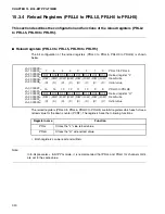
15.3.2 PPG1/3/5 Operation Mode Control Register
(PPGC1/PPGC3/PPGC5)
This section describes the configuration and functions of the PPG1/PPG3/PPG5
operation mode control register (PPGC1/PPGC3/PPGC5).
■
PPG1/PPG3/PPG5 operation mode control register (PPGC1/PPGC3/PPGC5)
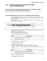
The PPG1/PPG3/PPG5 operation mode control register (PPGC1/PPGC3/PPGC5) is used to
select the channel 1/3/5 operation mode, control pin output, and select the count clock. It is also
used for trigger control.
The bit configuration of the PPG1/PPG3/PPG5 operation mode control register (PPGC1/
PPGC3/PPGC5) is shown below.
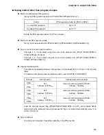
The functions of the bits in the PPG1/PPG3/PPG5 operation mode control register (PPGC1/
PPGC3/PPGC5) are described below.
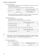
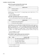
[bit15] PEN1: ppg Enable (operation enable)
This bit is used to select the PPG operation mode.
•
When this bit is set to "1", PPG count starts.
•
This bit is initialized to "0" at reset.
•
Reading and writing are allowed.
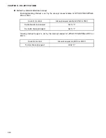
[bit13] PE10: ppg output Enable 10 (PPG1/PPG3/PPG5 output pin enable)
This bit is used to allow or prohibit pulse output to the pulse output external pin PPG1/PPG3/
PPG5.
•
This bit is initialized to "0" at reset.
•
Reading and writing are allowed.
15
14
1
3
12 11 10 9
8
PPGC1/
3
/5
PEN1
-
PE10
PIE1
PUF1
MD1
MD0
Re
s
erved
Oper
a
tion mode control regi
s
ter
(R/W)
(-)
(R/W) (R/W) (R/W) (R/W) (R/W) (-)
Re
a
d/write
(0) (X) (0) (0) (0) (0) (0) (1) Initi
a
l v
a
l
u
e
ch.1 0000
3
B
H
ch.
3
0000
3
D
H
ch.5 0000
3
F
H
PEN1
Operation state
0
Operation stop ("L" level output is retained)
1
PPG operation enabled
PE10
Operation state
0
General-purpose port pin (pulse output prohibited)
1
PPG1/PPG3/PPG5 pulse output (pulse output allowed)
Summary of Contents for MB90480 Series
Page 2: ......
Page 4: ......
Page 10: ...vi ...
Page 128: ...106 CHAPTER 4 RESET ...
Page 174: ...152 CHAPTER 6 LOW POWER CONSUMPTION MODE ...
Page 198: ...176 CHAPTER 7 MODE SETTING ...
Page 220: ...198 CHAPTER 9 TIMEBASE TIMER ...
Page 238: ...216 CHAPTER 11 WATCH TIMER ...
Page 280: ...258 CHAPTER 12 16 BIT INPUT OUTPUT TIMER ...
Page 406: ...384 CHAPTER 17 8 10 BIT A D CONVERTER ...
Page 478: ...456 CHAPTER 20 CHIP SELECTION FACILITY ...
Page 494: ...472 CHAPTER 21 ADDRESS MATCH DETECTION FUNCTION ...
Page 498: ...476 CHAPTER 22 ROM MIRROR FUNCTION SELECTION MODULE ...
Page 526: ...504 CHAPTER 23 2M 3M BIT FLASH MEMORY ...
Page 536: ...514 CHAPTER 24 EXAMPLES OF MB90F481B MB90F482B MB90F488B MB90F489B SERIAL PROGRAMMING ...
Page 570: ...548 CHAPTER 25 PWC TIMER ONLY MB90485 SERIES ...
Page 688: ......

