background image

GENERAL

1-13

1.8

Notes on Handling Devices

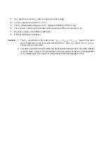
(1) Be careful not to exceed the maximum rated voltage (Prevention of latch up).

For a CMOS IC, latch-up may occur if a voltage higher than Vcc or a voltage lower than Vss is applied to the

I/O pin other than medium-/high-voltage withstand  I/O  pins, or when a voltage that exceeds the rated

voltage is applied between Vcc and Vss.

Latch up rapidly increases the power current, and the device may be destroyed by heat.

When using the device, take care not to exceed the maximum rating.  Also, take care that the analog power

(AVcc) and the analog input do not exceed the digital power (Vcc) when turning the AC/DC power on or off.

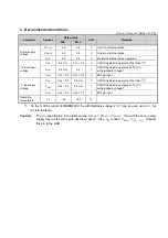
(2) Design the device so the supply voltage is as stable as possible.

A sudden change in the power voltage may cause a malfunction even within the operating assurance range

of the VCC power supply voltage.  For safety, the VCC ripple (p-p) of the commercial frequency (50/60

MHz) must be 10% or less of the standard VCC value, and the transient fluctuation at instantaneous power

switching must be 0.1 V/ms or less.  Also, take countermeasures to power noise, etc.

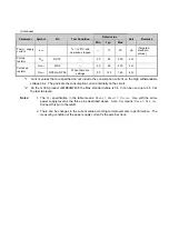
(3) Notes at power-on

The voltage rise time at power-on must be 50 µs or more (0.2 to 2.7 V).

(4) Setting unused input pins

Leaving unused input pins open may cause a malfunction.  Therefore, these pins must be set to the pull-

up or pull-down state.

(5)  Handling of power pins for A/D converter

Even when the A/D converter is not used, connect the pins so that the following relationships are

established:  AV

CC

 = V

CC

, AV

SS

 = V

SS

.

(6) Notes on using external clock

Even when an external clock is used, the oscillation stabilization wait time is required at the power-on reset

or the cancellation of the stop mode.  In this case, drive the X0 pin only and leave the X1 pin open.

     Example of using external clock

X0

X1
MB90M405 Series

OPEN

Summary of Contents for MB90M405

Page 1: ...FUJITSU SEMICONDUCTOR MICROCONTROLLER MB90M405 F2 MC 16LX FAMILY 16 BIT MICROCONTROLLERS HARDWARE MANUAL ABSTRACTS 查询MB90M405供应商 捷多邦 专业PCB打样工厂 24小时加急出货 ...

Page 2: ...ii ...

Page 3: ...nder the copy right patent right to trademarks claimed and owned by Fujitsu 4 Fujitsu reserved the right to change products or specifications without notice 5 No part of this publication may be copied or reproduced in any form or by any means or transferred to any third party without prior written consent of Fujitsu 6 The products described in this document are not intended for use in equipment re...

Page 4: ...ts of each register from the address register abbreviation register name and resource macro name Use the register map index at searching for the register function when designing a resource macro 2 Pin function index The pin function index is similar to the explanation of the pin function and it allows serch for the block diagram of each resource macro the explanation of the pin function and notes ...

Page 5: ...s 1 4 1 3 Product Lineup 1 5 1 4 Block Diagram 1 6 1 5 Pin Assignment 1 7 1 6 Pin Description 1 8 1 7 I O Circuit Type 1 11 1 8 Notes on Handling Devices 1 13 1 9 Clock Supply Map 1 15 1 10 Low Power Consumption Mode 1 16 1 GENERAL ...

Page 6: ...MB90M405 F2 MC 16LX FAMILY HARDWARE MANUAL 1 2 ...

Page 7: ...ing the original oscillation by 4 and Vcc 3 V It is possible to generate an external output as a clock output by dividing the original oscillation by 16 32 64 or 128 Maximum memory space 16 Mbytes 24 bit addressing in memory space Instruction system suited for controller Applicable data types bit byte word long word Various addressing modes 23 types High code efficiency High precision operation wi...

Page 8: ...f the shift clock level can be selected arbitrarily MSB or LSB DTP external interrupt 4 channels Start extended intelligent I O services by an external input and generate an external interrupt Delayed interrupt generation module A task switching interrupt request is generated 8 10 bit A D converter 16 channel 8 or 10 bit resolution can be selected FL controller Enables FL driver control The auto d...

Page 9: ...r control the dimmer can be set for both digits and segments Serial I O UART Can also be used as the clock synchronous method extended I O serial A dedicated baud rate generator is built in Four channels are built in two channels also serve as UART channels 16 bit reload timer 16 bit reload timer operation Toggle output or one shot output can be selected An event count function can be selected Thr...

Page 10: ...D2 1 0 16 bit free run timer 16 bit input capture ch 0 1 16 bit output compare I 2 C Interface 16 bit reload timer ch 0 1 2 FMC 16LX Bus PA0 AN0 TMCK PA1 AN1 PA2 AN2 PA3 AN3 PA4 AN4 PA5 AN5 PA6 AN6 PA7 AN7 PB0 AN8 PB1 AN9 PB2 AN10 PB3 AN11 SI2 PB4 AN12 SC2 TIN PB5 AN13 SO2 TO PB6 AN14 INT3 PB7 AN15 INT2 P80 IC0 INT0 P81 IC1 INT1 P82 SI0 P83 SC0 P84 SO0 P85 SI1 P86 SI2 P87 SI3 P90 SDA SO3 P91 SCL S...

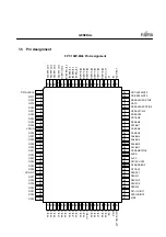
Page 11: ... 47 FIP59 48 VKK 49 MD0 50 MD1 VDD VFT 60 59 58 57 56 55 54 53 52 51 P82 SI0 P81 IC1 INT1 P80 IC0 INT0 MD2 P86 SC1 P85 SI1 P84 SO0 P83 SC0 P90 SDA SO3 P87 SO1 70 69 68 67 66 65 64 63 62 61 PA0 AN0 TMCK AVSS AVCC P91 SCL SC3 PA4 AN4 PA3 AN3 PA2 AN2 PA1 AN1 PA6 AN6 PA5 AN5 80 79 78 77 76 75 74 73 72 71 PB2 AN10 PB1 AN9 PB0 AN8 PA7 AN7 PB5 AN13 SO2 TO0 RSTX PB4 AN12 SC2 TIN0 PB3 AN11 SI2 PB7 AN15 INT...

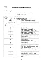
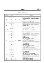
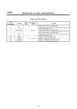
Page 12: ...ccepted when it is enabled by the EN1 bit P82 General purpose I O port 54 SI0 Serial data input pin for serial I O channel 0 This pin is always effective when channel 0 is under input operation P83 General purpose I O port 55 SC0 Serial clock I O pin for serial I O channel 0 This pin is effective when the channel 0 clock output is enabled P84 General purpose I O port 56 SO0 Serial data output pin ...

Page 13: ...el 2 is under input operation PB4 General purpose I O port AN12 Analog input pin 12 for the A D converter This function is effective when the analog input specification is enabled using ADER SC2 Serial clock I O pin for serial I O channel 2 This pin is effective when the channel 2 clock output is enabled 76 TIN0 External clock input pin for reload timer channel 0 This pin is enabled when the exter...

Page 14: ... 50 MD1 VDD VFT Input pin for specifying the operating mode Connect this pin to Vcc This pin also serves as the VDD VFT pin 51 MD2 B Mode pin Input pin for specifying the operating mode Connect this pin to Vss Also always switch this pin to Vcc at boot programming to flash memory 11 42 VSS IO Power 0 V GND input pins for I O 23 VDD FIP Power 3 V Vcc input pin for the FIP 81 VSS CPU Power 0 V GND i...

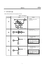
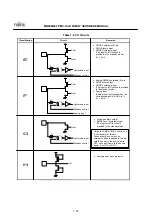
Page 15: ...ithstand port output IOL 25 mA D P ch open drain output High voltage withstand port output IOL 12 mA Circuit Remarks Xout Pout RKK VKK When using the pin as a normal port connect a diode clamp etc to prevent application of VKK voltage to the pin at output of the L level see Handling notes Pout RKK VKK When using the pin as a normal port connect a diode clamp etc to prevent application of VKK volta...

Page 16: ...is input The input cutoff function is provided in the standby mode Analog input Analog input is effective when the corresponding bit of ADER is 1 IOL 4 mA Classification Circuit Remarks Standby control Pout Hysteresis input Standby control Nout Analog input R Hysteresis input Standby control Nout R IN Unlike the CMOS I O pin there is no P ch transistor at this pin Consequently even when an externa...

Page 17: ...ing assurance range of the VCC power supply voltage For safety the VCC ripple p p of the commercial frequency 50 60 MHz must be 10 or less of the standard VCC value and the transient fluctuation at instantaneous power switching must be 0 1 V ms or less Also take countermeasures to power noise etc 3 Notes at power on The voltage rise time at power on must be 50 µs or more 0 2 to 2 7 V 4 Setting unu...

Page 18: ...and Vss 8 Application sequence for power analog inputs for A D converter Apply the digital power Vcc first and then apply the power AVcc and analog inputs AN0 to AN15 for the A D converter Disconnect the power and analog inputs for the A D converter first and then disconnect the digital power Vcc Also do not allow the input voltage to exceed AVcc even when using a pin shared with an analog input a...

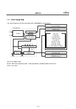
Page 19: ...lock by 2 PCLK PLL clock Clock generator Oscillator Selector Timer clock divider Time base timer PLL Multiplication circuit PCLK Selector Divide by 2 circuit MCLK HCLK 1 2 3 4 Watchdog timer Resources FL Controller 16 bit reload timer 10 bit A D converter 8 bit serial I O 6 bit free run timer 16 bit input capture 16 bit output compare I2 C Communications interface CPU F2 MC 16LX ROM RAM memory X0 ...

Page 20: ... Operates Operates PLL Sleep Operates Operates Stops Operates Operates Main sleep Operates Stops Stops Operates Operates Pseudo time Operates Stops Stops Stops Operates Stop Stops Stops Stops Stops Stops In the above table the power consumption decreases as the operating mode goes down from the top of the table In the PLL Run mode operation is performed on the PCLK generated by multiplying the ori...

Page 21: ...4 5 L level avg output current IOLAV 4 mA Average value Operating current Operating rate 5 L level max overall output current ΣIOL 100 mA 5 L level avg overall output current ΣIOLAV 50 mA Average value Operating current Operating rate 5 IOH 15 mA 4 5 IOHFIP1 27 mA FIP00 to FIP33 pins H level max output current IOHFIP2 14 mA FIP34 to FIP59 pIns H level avg output current IOHAV 4 mA Average value Op...

Page 22: ...s 6 FIP00 to FIP59 pins are targeted Cautions 1 The VCC specification in the table means VDD FIP VDD VFT VCC CPU Use with the same power supply level as the three pins described above Also VSS means VSS IO VSS CPU Connect this pin to the GND 2 This device contains circuity to protect the inputs against damage due to high static voltages or electric fields However it is advised that normal precauti...

Page 23: ...input voltage VIHM Vcc 0 3 Vcc 0 3 V MD pin input VILS Vss 0 3 0 2 Vcc V CMOS Hysterisis input pins other than I 2 C VILS2 Vss 0 3 0 2 Vcc V CMOS Hysterisis input pins of I 2 C 5 V withstandable voltage 1 L level input voltage VILM Vss 0 3 Vss 0 3 V MD pin input Operation temperature TA 40 85 C 1 On the 1st ES product of MB90MF408 the withstandable voltage is 3 V can be used up to 4 5 V at the tes...

Page 24: ...rent IIL Input pins other than FIP00 59 VCC 3 0 V VS VI VCC 5 1 5 µA ILO3 FIP00 to FIP33 VCC 3 3 V VCC 43 VI VCC 20 µA Output leak current ILO2 FIP34 to FIP59 VCC 3 3 V VCC 43 VI VCC 10 µA Vcc 3 3 V and internal operation at 16 MHz and normal operation 32 40 mA MB90M407 8 argeted standard values 1 Vcc 3 3 V and internal operation at 16 MHz and A D operation 37 45 mA MB90M407 8 targeted standard va...

Page 25: ...rent on the high withstandable voltage pins They indicate the consumption current internally on the circuit 2 On the 1st ES product of MB90MF408 the Max standard value is 3 6 V can be used up to 4 5 V at the test lab level Notes 1 The VCC specification in the table means VDD FIP VDD VFT VCC CPU Use with the same power supply level as the three pins described above Also VSS means VSS IO VSS CPU Con...

Page 26: ... 3 1 5 3 0 3 6 Power supply voltage Vcc V PLL operating guaranteed range Relationship between original oscillation frequency and internal operation clock frequency Original Oscillating Clock fCP MHz 4 multipulation 3 multipulation 2 multipulation 1 multipulation Non multipulation 8 16 3 8 4 16 12 Internal clock f CP MHz 12 6 4 3 2 1 5 6 9 ...

Page 27: ...cc 5 mA Power supply current IAH AVcc 5 µA 1 IR AVcc 100 200 µA Reference voltage supply current IRH AVcc 5 µA 1 Channel differences AN0 to AN15 4 LSB 1 When not operating A D converter this is the current VCC CPU AVCC 3 3 V when the CPU is stopped 2 tCP means 1 internal operating frequency When the internal operating frequency is 16 MHz tCP is 1 16 MHz 62 5 ns Notes 1 The reference L value is fix...

Page 28: ...d VCC CPU value in commercial frequencies 50 to 60 Hz and so that transient variation is below 0 1 V ms in sudden changes during power switchovers Precautions when turning on the power supply Ensure a minimum of 50 µs between 0 2 to 2 7 V for voltage rise times when turning on the power supply to prevent malfunction of the built in power reduction circuit Handling of unused input pins Leaving unus...

Reviews: