MB95630H Series
194
FUJITSU SEMICONDUCTOR LIMITED
MN702-00009-1v0-E
CHAPTER 13 INTERRUPT PIN SELECTION CIRCUIT
13.5 Register
[bit2] UI0: UI0 interrupt pin select bit
This bit determines whether to select the UI0 pin as an interrupt input pin.
Writing "0" to this bit deselects the UI0 pin as an interrupt input pin, and the interrupt pin selection circuit
treats the UI0 pin input as being fixed at "0".
Writing "1" to this bit selects the UI0 pin as an interrupt input pin and the circuit passes the UI0 pin input to
INT00 (ch. 0) of the external interrupt circuit. In this case, the input signal to the UI0 pin can generate an
external interrupt if INT00 (ch. 0) operation is enabled in the external interrupt circuit.
[bit1] UCK0: UCK0 interrupt pin select bit
This bit determines whether to select the UCK0 pin as an interrupt input pin.
Writing "0" to this bit deselects the UCK0 pin as an interrupt input pin, and the interrupt pin selection circuit
treats the UCK0 pin input as "0".
Writing "1" to this bit selects the UCK0 pin as an interrupt input pin and the circuit passes the UCK0 pin
input to INT00 (ch. 0) of the external interrupt circuit. In this case, the input signal to the UCK0 pin can
generate an external interrupt if INT00 (ch. 0) operation is enabled in the external interrupt circuit.
[bit0] TRG1: TRG1 interrupt pin select bit
This bit determines whether to select the TRG1 pin as an interrupt input pin.
Writing "0" to this bit deselects the TRG1 pin as an interrupt input pin, and the interrupt pin selection circuit
treats the TRG1 pin input as being fixed at "0".
Writing "1" to this bit selects the TRG1 pin as an interrupt input pin and the circuit passes the TRG1 pin
input to INT00 (ch. 0) of the external interrupt circuit. In this case, the input signal to the TRG1 pin can
generate an external interrupt if INT00 (ch. 0) operation is enabled in the external interrupt circuit.
When any of these bits (except undefined bits) is set to "1" and the operation of INT00 (ch. 0)
of the external interrupt circuit is enabled in standby mode of this device, the selected pin is
enabled to perform input operation. The device wakes up from the standby mode when a valid
edge pulse is input to the selected pin. For detail of the standby mode, see "3.5 Operations in
Low Power Consumption Mode (Standby Mode)".
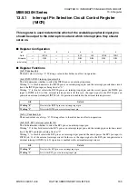
bit2
Details
Writing "0"
Deselects the UI0 pin as an interrupt input pin.
Writing "1"
Selects the UI0 pin as an interrupt input pin.
bit1
Details
Writing "0"
Deselects the UCK0 pin as an interrupt input pin.
Writing "1"
Selects the UCK0 pin as an interrupt input pin.
bit0
Details
Writing "0"
Deselects the TRG1 pin as an interrupt input pin.
Writing "1"
Selects the TRG1 pin as an interrupt input pin.

