MB95630H Series
378
FUJITSU SEMICONDUCTOR LIMITED
MN702-00009-1v0-E
CHAPTER 21 MULTI-PULSE GENERATOR
21.1 Overview
21.1
Overview
The multi-pulse generator consists of a 16-bit PPG timer, a 16-bit reload timer
and a waveform sequencer. By using the waveform sequencer, 16-bit PPG timer
output signal can be directed to multi-pulse generator output (OPT5 to OPT0)
according to the input signal of the multi-pulse generator (SNI2 to SNI0).
Meanwhile, the OPT5 to OPT0 output signal can be hardware terminated by
DTTI input in case of emergency. The OPT5 to OPT0 output signals are
synchronized with the PPG signal in order to eliminate the unwanted glitch.
For details of the 16-bit PPG timer and the 16-bit reload timer, see "CHAPTER
19 16-BIT PPG TIMER" and "CHAPTER 20 16-BIT RELOAD TIMER" respectively.
■
Function of Waveform Sequencer
●
Output signal control
With waveform sequencer, it is possible to generate 16-bit PPG timer waveform output and DC
chopper waveform output at the multi-pulse generator output (OPT5 to OPT0).
•
When an effective edge of the input signal from multi-pulse generator position detect input
(SNI2 to SNI0) or when an underflow occurs in the 16-bit reload timer or when the
OPDBRH0 and OPDBRL0 registers are set, data of one pair of the 16-bit MPG output data
buffer register (upper/lower) (OPDBRHx/OPDBRLx) is loaded to the 16-bit MPG output
data register (upper) (OPDUR) and the 16-bit MPG output data register (lower) (OPDLR).
•
The 16-bit MPG output data register (upper/lower) (OPDUR/OPDLR) determines the 16-
bit PPG timer output to which OPT output (OPT5 to OPT0). By loading different 16-bit
MPG output data buffer register (upper/lower) (OPDBRHx/OPDBRLx) to the 16-bit MPG
output data register (upper/lower) (OPDUR/OPDLR), various combination of OPT outputs
(OPT5 to OPT0) can be obtained.
•
Therefore, the 16-bit PPG timer output can be presented/absented at multi-pulse generator
output (OPT5 to OPT0) or switch the PPG timer output signal from one OPT output to
another OPT output according to the sequence set in the 16-bit MPG output data register
(upper/lower) (OPDUR/OPDLR) and 12 pairs of 16-bit MPG output data buffer register
(upper/lower) (OPDBRHx/OPDBRLx). Meanwhile, the 16-bit reload timer can insert a
delay when switch OPT output.
•
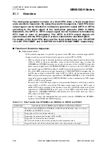
Table 21.1-1 shows the combination the data transfer from the OPDBRHx and OPDBRLx
registers to the OPDUR and OPDLR registers.
Table 21.1-1 Data Transfer from OPDBRHx and OPDBRLx to OPDUR and OPDLR
Combination
Data transfer from OPDBRHx and OPDBRLx to OPDUR and OPDLR
1
Data transfer from OPDBRH0 and OPDBRL0 to OPDUR and OPDLR after values are written to
OPDBRH0 and OPDBRL0 by software.
2
Triggered by the16-bit reload timer underflow.
3
Triggered by the position detection input (SNI2 to SNI0).
4
Triggered by the 16-bit reload timer underflow.
The 16-bit reload timer is started by the position detection comparison circuit.
5
Triggered either by the 16-bit reload timer underflow, or by the position detection input.


