MB95630H Series
386
FUJITSU SEMICONDUCTOR LIMITED
MN702-00009-1v0-E
CHAPTER 21 MULTI-PULSE GENERATOR
21.2 Block Diagram
●
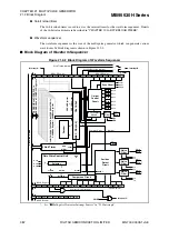
16-bit MPG timer buffer register (upper) (TMBUR) and 16-bit MPG timer buffer register
(lower) (TMBLR)
The 16-bit MPG timer buffer register (upper) (TMBUR) and the 16-bit MPG timer buffer
register (lower) (TMBLR) are used store the value of the 16-bit up counter when a write timing
interrupt or position detect interrupt occurs.
●
16-bit MPG timer control status register (TCSR)
The 16-bit MPG timer control status register (TCSR) is used to control the operation of the 16-
bit timer such as the clock frequency, enable/disable the interrupt.
■
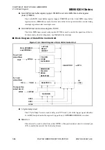
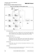
Block Diagram of Data Write Control Unit
Figure 21.2-4 Block Diagram of Data Write Control Unit
●
1-Cycle delay circuit
The 1-Cycle Delay Circuit is used to delay one CPU clock cycle of the trigger signal when the
16-bit MPG output data buffer register 0 (upper/lower) (OPDBRH0/OPDBRL0) is written.
●
Selector 0
The selector 0 is used to select from either WTIN1 of the position detect circuit or external pin
(TI1) to enable the count of the 16-bit reload timer.
1-CYCLE
TIN
From 16-bit
DELAY
TIN0O
WTIN0
WTO
Write OPDBRH0
SELECTOR 1
FALLING
EDGE
RISING AND
FALLING
DECODER
WTIN1
OPS2
OPS1
SELECTOR 0
EDGE
DETECTOR
DETECTOR
CIRCUIT
OPS0
TOUT
To 16-bit
From position
WTIN1
reload timer
reload timer
detect circuit
Pin
TI1
and OPDBRL0


