MB95630H Series
394
FUJITSU SEMICONDUCTOR LIMITED
MN702-00009-1v0-E
CHAPTER 21 MULTI-PULSE GENERATOR
21.5 Operations
21.5.1
Operation of Position Detection
This section describes the operation of the Position Detection Circuit. When
the effective position is detected, a Data Write Timing Output (WTIN1) will be
generated to the data write control unit and a Position Detect Interrupt is
generated if the OPCLR:PDIE is set to "1".
■
Operation of Position Detection
The WTIN1 signal is generated by the Position Detection Circuit under the following
conditions:
•
A comparison match between SNI2 to SNI0 and RDA[2:0], which is triggered by any
effective edge of SNI2 to SNI0.
•
A detection of effective edge at SNIx which is enabled by the corresponding SEEx bit.
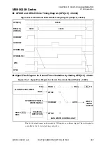
When the CMPE bit in the 16-bit MPG input control register (upper) (IPCUR) is set to "0",
only the edge detection of SNIx pins enabled by the SEE[2:0] bits will engage in the edge
detection operation for the position detection. For instance, when only the SEE0 bit is set to
"1", the input edge to the pin SNI0 is in effect, the data write output signal is generated only
when an effective edge is detected at the SNI0 pin. See Figure 21.5-3 for the timing diagram of
the edge detection when CMPE = 0.
When the CMPE bit in the 16-bit MPG input control register (upper) (IPCUR) is set to "1", the
SNI2 to SNI0 pins will be engaged in the comparison operation with the RDA[2:0] bits. The
comparison is triggered by any edge change at the SNI2 to SNI0 pins. See Figure 21.5-4 for the
timing diagram of the edge detection when CMPE = 1.
■
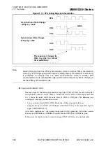
Edge Detection Timing Diagram (CMPE = 0)
Figure 21.5-3 Edge Detection Timing Diagram (CMPE = 0)
0b10
0b01
0b11
WTIN1
CPE1,
CPE0
SNI0
SNI1
SNI2
CMPE
RISING EDGE
DETECTION
FALLING EDGE
DETECTION
BOTH EDGES
DETECTION

