MB95630H Series
MN702-00009-1v0-E
FUJITSU SEMICONDUCTOR LIMITED
31
CHAPTER 3 CLOCK CONTROLLER
3.3 Registers
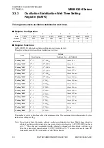
[bit3:0] MWT[3:0]: Main clock oscillation stabilization wait time select bits
These bits set the main clock oscillation stabilization wait time.
The number of cycles in the above table is the minimum value. The maximum value is the number of cycles
in the above table plus 1/F
CH
.
Note: Do not modify these bits during main clock oscillation stabilization wait time. Modify them when the
main clock oscillation stabilization bit in the system clock control register 2 (SYCC2:MRDY) has
been set to "1". These bits can be modified when the main clock is stopped with the main clock
oscillation stop bit in the system clock control register 2 (SYCC2:MOSCE) set to "0" in main CR
clock mode, main CR PLL clock mode, subclock mode, or sub-CR clock mode.
bit3:0
Details
No. of cycles
Main clock (F
CH
) = 4 MHz
Writing "1111"
2
14
- 2
(2
14
- 2)/F
CH
About 4.10 ms
Writing "1110"
2
13
- 2
(2
13
- 2)/F
CH
About 2.05 ms
Writing "1101"
2
12
- 2
(2
12
- 2)/F
CH
About 1.02 ms
Writing "1100"
2
11
- 2
(2
11
- 2)/F
CH
About 511.5 µs
Writing "1011"
2
10
- 2
(2
10
- 2)/F
CH
About 255.5 µs
Writing "1010"
2
9
- 2
(2
9
- 2)/F
CH
About 127.5 µs
Writing "1001"
2
8
- 2
(2
8
- 2)/F
CH
About 63.5 µs
Writing "1000"
2
7
- 2
(2
7
- 2)/F
CH
About 31.5 µs
Writing "0111"
2
6
- 2
(2
6
- 2)/F
CH
About 15.5 µs
Writing "0110"
2
5
- 2
(2
5
- 2)/F
CH
About 7.5 µs
Writing "0101"
2
4
- 2
(2
4
- 2)/F
CH
About 3.5 µs
Writing "0100"
2
3
- 2
(2
3
- 2)/F
CH
About 1.5 µs
Writing "0011"
2
2
- 2
(2
2
- 2)/F
CH
About 0.5 µs
Writing "0010"
2
1
- 2
(2
1
- 2)/F
CH
0.0 µs
Writing "0001"
2
1
- 2
(2
1
- 2)/F
CH
0.0 µs
Writing "0000"
2
1
- 2
(2
1
- 2)/F
CH
0.0 µs


