MB95630H Series
534
FUJITSU SEMICONDUCTOR LIMITED
MN702-00009-1v0-E
CHAPTER 25 DUAL OPERATION FLASH MEMORY
25.2 Sector/Bank Configuration
25.2
Sector/Bank Configuration
This section shows the sector/bank configuration of the Flash memory.
■
Sector/Bank Configuration of Dual Operation Flash Memory
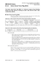
Figure 25.2-1 shows the sector configuration of the Dual operation Flash memory. The upper
and lower addresses of each sector are shown in the figure.
●
Bank configuration
The lower bank of the Flash memory is SA0 and SA1 and the upper bank SA2.
Figure 25.2-1 Sector/Bank Configuration of Dual Operation Flash Memory
Flash memory
(8 Kbyte)
Flash memory
(12 Kbyte)
Flash memory
(20 Kbyte)
Flash memory
(36 Kbyte)
CPU
address
SA0: 2 Kbyte
SA0: 2 Kbyte
SA0: 2 Kbyte
SA0: 2 Kbyte
0x1000
Lower bank
0x17FF
SA1: 2 Kbyte
SA1: 2 Kbyte
SA1: 2 Kbyte
SA1: 2 Kbyte
0x1800
0x1FFF
Vacant
Vacant
Vacant
Vacant
0x2000
0x7FFF
SA2: 32 Kbyte
0x8000
Upper bank
0xBFFF
SA2: 16 Kbyte
0xC000
0xDFFF
SA2: 8 Kbyte
0xE000
0xEFFF
SA2: 4 Kbyte
0xF000
0xFFFF


