MB95630H Series
560
FUJITSU SEMICONDUCTOR LIMITED
MN702-00009-1v0-E
CHAPTER 25 DUAL OPERATION FLASH MEMORY
25.8 Registers
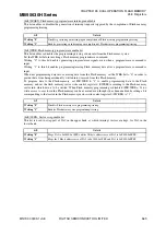
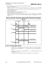
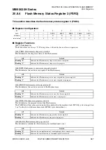
[bit5] PTIEN: PGMTO interrupt enable bit
This bit enables or disables the generation of interrupt requests triggered by the failure of Flash memory
programming.
[bit4] PGMTO: PGMTO interrupt request flag bit
This bit indicates that Flash memory programming has failed.
When Flash memory programming fails, the PGMTO bit is set to "1" upon completion of the Flash memory
automatic algorithm. Afterward, further Flash memory programming/erasing is disabled. Writing a reset
command can make the Flash memory return to the normal command state.
An interrupt request is generated when the PGMTO bit is set to "1", provided that generating an interrupt
request upon failure of Flash memory programming has been enabled (FSR2:PTIEN = 1).
Writing "0" to this bit clears it.
Writing "1" to this bit has no effect on operation.
When read by the read-modify-write (RMW) type of instruction, this bit always returns "1".
[bit3] EEIEN: ERSEND interrupt enable bit
This bit enables or disables the generation of interrupt requests triggered by the completion of Flash memory
sector erase.
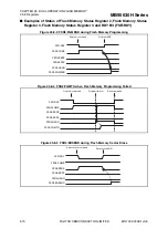
[bit2] ERSEND: ERSEND interrupt request flag bit
This bit indicates the completion of Flash memory sector erase.
The ERSEND bit is set to "1" upon completion of the Flash memory automatic algorithm.
An interrupt request is generated when the ERSEND bit is set to "1", provided that generating an interrupt
request upon completion of Flash memory sector erase has been enabled (FSR2:EEIEN = 1).
When the ERSEND bit is set to "0" after Flash memory sector erase is completed, further Flash memory
programming/erasing is disabled. Writing a reset command can make the Flash memory return to the normal
command state.
When Flash memory sector erase fails (FSR3:HANG = 1), the ERSEND bit is cleared to "0".
Writing "0" to this bit clears it.
Writing "1" to this bit has no effect on operation.
When read by the read-modify-write (RMW) type of instruction, this bit always returns "1".
bit5
Details
Writing "0"
Disables the interrupt request upon failure of Flash memory programming (FSR2:PGMTO = 1).
Writing "1"
Enables the interrupt request upon failure of Flash memory programming (FSR2:PGMTO = 1).
bit4
Details
Reading "0"
Indicates that the device is in the command input wait state or Flash memory programming is in
progress.
Reading "1"
Indicates that Flash memory programming has failed.
Writing "0"
Clears this bit.
Writing "1"
Has no effect on operation.
bit3
Details
Writing "0"
Disables the interrupt request upon completion of Flash memory sector erase
(FSR2:ERSEND = 1).
Writing "1"
Enables the interrupt request upon completion of Flash memory sector erase
(FSR2:ERSEND = 1).
bit2
Details
Reading "0"
Indicates that the device is in the command input wait state or Flash memory erase is in progress.
Reading "1"
Indicates that Flash memory sector erase has been completed.
Writing "0"
Clears this bit.
Writing "1"
Has no effect on operation.


