MB95630H Series
228
FUJITSU SEMICONDUCTOR LIMITED
MN702-00009-1v0-E
CHAPTER 14 LIN-UART
14.6 Operations of LIN-UART and LIN-UART
Setting Procedure Example
●
Clock supply
In clock synchronous mode (normal), the number of transmit/receive data bits must be equal to
the number of clock cycles. When the start/stop bits are enabled, the number of clock cycles
must be equal to the sum of the transmit/receive data bits and the added start/stop bits.
With the serial clock transmission side having been selected (ECCR:MS = 0), when the serial
clock output is enabled (SMR:SCKE = 1), a synchronous clock is automatically output during
transmission/reception. When the serial clock reception side (ECCR:MS = 1) is selected or the
serial clock output is disabled (SMR:SCKE = 0), clock cycles equal to the number of transmit/
receive data bits must be supplied from an external clock pin.
The clock signal must be kept at the mark level ("H") if serial data is not related to
transmission/reception.
●
Clock delay
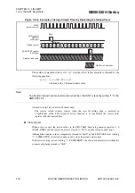
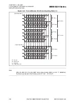
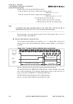
When the SCDE bit in the ECCR is set to "1", a delayed transmit clock is output as shown in
Figure 14.6-5. This function is required when the device on the reception side samples data at
the rising edge or falling edge of the serial clock.
Figure 14.6-5 Transmit Clock Delay (SCDE = 1)
●
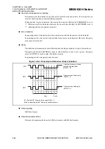
Clock inversion
When the SCES bit in the LIN-UART extended status register (ESCR) is "1", the LIN-UART
clock is inverted, and receive data is sampled at the falling edge of the LIN-UART clock. At
that time, the value of the serial data must become valid at the edge of the LIN-UART clock.
Write tr
a
n
s
mit d
a
t
a
Tr
a
n
s
mit/receive
clock (norm
a
l)
Tr
a
n
s
mit/receive d
a
t
a
1
D
a
t
a
L
S
B
M
S
B
M
a
rk level
Tr
a
n
s
mit clock
(
S
CDE = 1)
M
a
rk level
M
a
rk level
Receive d
a
t
a
sa
mple edge (
S
CE
S
= 0)
0
1
1
0
1
0
0


