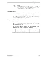
5.2 Logical Interface
C141-E145-02EN
5-7
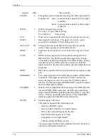
5.2.1 I/O registers
Communication between the host system and the device is done through input-
output (I/O) registers of the device.
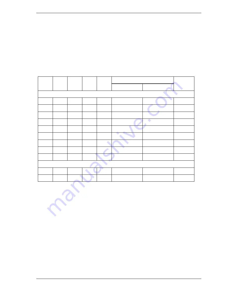
These I/O registers can be selected by the coded signals, CS0-, CS1-, and DA0 to
DA2 from the host system. Table 5.2. shows the coding address and the function
of I/O registers.
Table 5.2 I/O registers
I/O registers
Read operation
Write operation
Command block registers
L
H
L
L
L
Data
Data
X’1F0’
L
H
L
L
H
Error Register
Features
X’1F1’
L
H
L
H
L
Sector Count
Sector Count
X’1F2’
L
H
L
H
H
Sector Number
Sector Number
X’1F3’
L
H
H
L
L
Cylinder Low
Cylinder Low
X’1F4’
L
H
H
L
H
Cylinder High
Cylinder High
X’1F5’
L
H
H
H
L
Device/Head
Device/Head
X’1F6’
L
H
H
H
H
Status
Command
X’1F7’
L
L
X
X
X
(Invalid)
(Invalid)
—
Control block registers
H
L
H
H
L
Alternate Status
Device Control
X’3F6’
H
L
H
H
H
—
—
X’3F7’
Notes:
1.
The Data register for read or write operation can be accessed by 16 bit data
bus (DATA0 to DATA15).
2.
The registers for read or write operation other than the Data registers can be
accessed by 8 bit data bus (DATA0 to DATA7).
3.
When reading the Drive Address register, bit 7 is high-impedance state.
4.
H indicates signal level High and L indicates signal level Low.
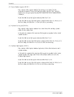
There are two methods for specifying the LBA mode. One method is to
specify the LBA mode with 28-bit address information, and the other is to
specify it with 48-bit address information (command of EXT system). If
the LBA mode is specified with 28-bit address information, the
Host I/O
address
DA0
DA1
DA2
CS1–
CS0–
Summary of Contents for MHR2010AT
Page 1: ...C141 E145 02EN MHR2040AT MHR2030AT MHR2020AT MHR2010AT DISK DRIVES PRODUCT MANUAL ...
Page 4: ...This page is intentionally left blank ...
Page 8: ...This page is intentionally left blank ...
Page 10: ...This page is intentionally left blank ...
Page 12: ...This page is intentionally left blank ...
Page 32: ...This page is intentionally left blank ...
Page 38: ...This page is intentionally left blank ...
Page 58: ...Theory of Device Operation 4 6 C141 E145 02EN Figure 4 3 Circuit Configuration ...
Page 188: ...Interface 5 114 C141 E145 02EN g d f f d e Figure 5 7 Normal DMA data transfer ...
Page 240: ...This page is intentionally left blank ...
Page 242: ...This page is intentionally left blank ...
Page 246: ...This page is intentionally left blank ...
Page 248: ...This page is intentionally left blank ...
Page 249: ......
Page 250: ......


