C141-E034-02EN
5 - 34
Table 5.5
Features register values and settable modes
Features Register
Drive operation mode
X‘02’
Enables the write cache function.
X‘03’
Specifies the transfer mode. Supports PIO mode 4, single word DMA mode 2,
and multiword DMA mode regardless of Sector Count register contents.
X‘55’
Disables read cache function.
X‘66’
Disables the reverting to power-on default settings after software reset.
X‘82’
Disables the write cache function.
X‘AA’
Enables the read cache function.
X‘BB’
Specifies the transfer of 4-byte ECC for READ LONG and WRITE LONG
commands.
X‘CC’
Enables the reverting to power-on default settings after software reset.
At power-on or after hardware reset, the default mode is the same as that is set with a value greater
than X‘AA’ (except for write cache). If X‘66’ is specified, it allows the setting value greater than
X‘AA’ which may have been modified to a new value since power-on, to remain the same even
after software reset.
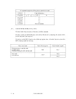
At command issuance (I/O registers setting contents)
1F7
H
(CM)
1
1
1
0
1
1
1
1
1F6
H
(DH)
×
×
×
DV
xx
1F5
H
(CH)
1F4
H
(CL)
1F3
H
(SN)
1F2
H
(SC)
1F1
H
(FR)
xx
xx
xx
xx or transfer mode
[See Table 5.6]
At command completion (I/O registers contents to be read)
1F7
H
(ST)
Status information
1F6
H
(DH)
×
×
×
DV
xx
1F5
H
(CH)
1F4
H
(CL)
1F3
H
(SN)
1F2
H
(SC)
1F1
H
(ER)
xx
xx
xx
xx
Error information
Summary of Contents for MPA3017AT
Page 1: ...C141 E034 02EN MPA3017AT MPA3026AT MPA3035AT MPA3043AT MPA3052AT DISK DRIVES PRODUCT MANUAL ...
Page 29: ...C141 E034 02EN 3 2 Figure 3 1 Dimensions ...
Page 44: ...C141 E034 02EN 4 5 Figure 4 2 MPA30xxAT Block diagram ...
Page 50: ...C141 E034 02EN 4 11 Figure 4 4 Read write circuit block diagram ...
Page 52: ...C141 E034 02EN 4 13 Figure 4 6 PR4 signal transfer ...


