background image

SK-96320-80PMC User Guide 

Chapter 3 Jumpers and Switches 

FMEMCU-UG-960010-11 

- 20 - 

© Fujitsu Microelectronics Europe GmbH 

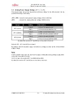
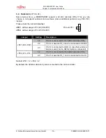
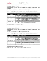
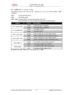
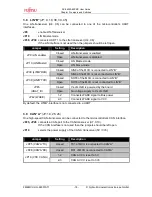
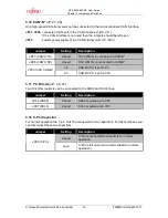
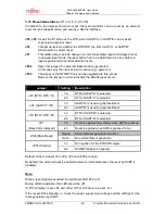
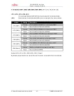
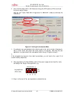
3.13 Reset-Generation 

(JP: 3, 4, 5, 7, 24, 35)


In addition to the internal Power-On reset, the microcontroller can be reset by an external 
reset circuit (Voltage Monitor) and also by a RS232 interface. 


JP3, JP5 

As well the DTR-line as the RTS-Line of UART”A” or UART”B” can be used  


to generate a system reset. 

JP4 

This jumper selects whether the DTR/RTS line from UART”A” or UART”B”  


will generate a system reset. 

JP7  

This solder jumper selects between normal (immediate) reset and delayed reset. 
 In delayed reset mode, the reset button has to be held down for 2 sec before a 
reset is generated to avoid accidental resets. 

JP24 

Open this jumper if no external Reset shall be generated.  


In this case only the internal reset is active (e.g.: power-on) 

JP35


The signal on the DTR/RTS line can be negated with this jumper.  


Remove the jumper in order to disable the RS232 reset circuit. 


Jumper 

Setting 

Description 

1-2 

DTR of UART”A” is selected 

JP3 (DTR / RTS “A”) 

2-3 

RTS of UART”A” is selected 

1-2 

UART”A” is used to generate Reset 

JP4 (UART”A”/”B”) 

2-3 

UART”B” is used to generate Reset 

1-2 

DTR of UART”B” is selected 

JP5 (DTR / RTS “B”) 

2-3 

RTS of UART”B” is selected 

1-2 

Reset is applied immediately when SW6 is pressed 

JP7 

(Reset imm./delayed) 

2-3 

Reset is applied when SW6 is pressed >2sec 

Closed 

External Reset generation is active 

JP24 (Main Reset) 

Open No 

external 

Reset 

generation 

1-2 

No negation for the DTR/RTS signal 

JP35 (Polarity) 

2-3 

DTR/RTS signal is negated 

Default: JP24 is closed; JP3, JP4, JP5 and JP35 are open 

By default, the external reset is enabled and set to immediate reset, the reset by UART is 
disabled. 


Note:

While a reset signal is asserted the red Reset-LED D14 is lit.  

During normal operation, this LED should be off!  

If JP35 (Polarity) is set, JP4 and either JP3 or JP5 have to be set, too. 

If the reset LED is steadily on, check the power supply input voltage and the settings for the 
reset-generation by UART. 

Summary of Contents for SK-96320-80PMC

Page 1: ...Fujitsu Microelectronics Europe User Guide FMEMCU UG 960010 11 F MC 16FX FAMILY EVALUATION BOARD SK 96320 80PMC USER GUIDE ...

Page 2: ...de Revision History FMEMCU UG 960010 11 2 Fujitsu Microelectronics Europe GmbH Revision History Date Issue 06 07 2007 V1 0 HWe DGo First Release 08 02 2008 V1 1 HWe China RoHS regulation added This document contains 34 pages ...

Page 3: ...m the date of receipt by the customer 2 Should a Product turn out to be defect Fujitsu Microelectronics Europe GmbH s entire liability and the customer s exclusive remedy shall be at Fujitsu Microelectronics Europe GmbH s sole discretion either return of the purchase price and the license fee or replacement of the Product or parts thereof if the Product is returned to Fujitsu Microelectronics Euro...

Page 4: ...1 15 3 5 UART A JP 1 2 31 16 3 6 UART B JP 6 8 32 16 3 7 LIN A JP 17 18 21 22 44 17 3 8 LIN B JP 9 10 38 39 45 18 3 9 CAN A JP 19 25 26 18 3 10 CAN B JP 27 28 19 3 11 I C Pull Up JP 46 47 19 3 12 C Pin Capacitor 19 3 13 Reset Generation JP 3 4 5 7 24 35 20 3 14 Buttons SW1 SW2 SW3 SW4 SW5 SW6 JP 12 14 16 20 23 24 21 4 PROGRAMMING THE INTERNAL FLASH MEMORY 22 4 1 Asynchronous Mode 22 4 2 Synchronou...

Page 5: ... Fujitsu Microelectronics Europe GmbH 5 FMEMCU UG 960010 11 5 7 VG96 connector X4 27 6 SILK PLOT OF THE BOARD 28 7 REVISION AND ERROR LIST 29 8 RELATED PRODUCTS 30 9 INFORMATION IN THE WWW 31 10 CHINA ROHS REGULATION 32 11 RECYCLING 34 ...

Page 6: ...M21 package or the MB2198 Emulator System with the Probe Cable MB2198 505 9 12V unregulated external DC power supply 5V and 3 3V onboard voltage regulators Power LEDs Onboard voltage supervisor monitor In Circuit serial Flash programming All resources available for evaluation All MCU pins routed to edge connectors 4 MHz main crystal 32 kHz crystal for sub clock operation Two RS232 two LIN and two ...

Page 7: ... by the unregulated supply input of the board so no additional supply is needed Two high speed CAN transceiver TLE6250GV33 are connected to the CAN interface of the MCU to allow easy connection to CAN networks All transceivers are fully 3 3V IO compatible to enable low voltage applications All pins of the microcontroller except the oscillator pins X0 1 A are connected to the edge connectors X1 and...

Page 8: ...nics Europe GmbH 1 3 1 Emulator System If the board is used as an emulator target board the microcontroller must be removed from the socket and the corresponding probe cable has to be mounted Series V Chip Probe cable NQ Pack HQ Pack MB96320 MB96V300B MB2198 505 NQPACK080SD ND HQPACK080SD ...

Page 9: ...e cable with the provided screws Do not use any other probe cable than MB2198 505 only Connect the probe cable to the MB2198 300 emulation Adapter Board Check all jumper settings of the evaluation board especially JP29 the Probe Cable and the Adapter Board When turning on the system be sure to use the following power up sequence 1 Power up the emulator main unit MB2198 01 2 Power up the adapter bo...

Page 10: ...AN A Solder JP 3 pin 1 2 I7 JP20 SW4 Jumper 2 pin Closed G7 JP21 LIN A TXD SIN7R Jumper 2 pin Open H10 JP22 LIN A RXD SOT7R Jumper 2 pin Open H10 JP23 SW5 Jumper 2 pin Closed F7 JP24 Reset Jumper 2 pin Closed F7 JP25 CAN A TXD TX1 Jumper 2 pin Closed H10 JP26 CAN A RXD RX1 Jumper 2 pin Closed I10 JP27 CAN B TXD TX2 Jumper 2 pin Closed I10 JP28 CAN B RXD RX2 Jumper 2 pin Closed I10 JP29 Vcc 5V 3V3 ...

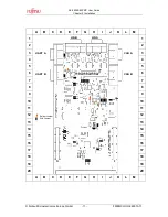
Page 11: ...electronics Europe GmbH 11 FMEMCU UG 960010 11 A B C D E F G H I J K L M 1 1 2 2 3 3 4 4 5 5 6 6 7 7 8 8 9 9 10 10 11 11 12 12 13 13 14 14 15 15 16 16 17 17 18 18 19 19 20 20 A B C D E F G H I J K L M UART A UART B CAN A CAN B LIN A LIN B Solder Jumper Std Jumper ...

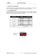
Page 12: ...efault setting MB96320 Series is shown with a grey shaded area 3 1 Operating Mode S2 The DIP switch S2 is used to set the operating mode of the KC Ensure that the mode pin settings correspond to the operation mode of the application For more detailed information please check the Hardware Manual of the microcontroller DIP switch Setting Logical value ON closed 1 high S2 1 MD0 OFF open 0 low ON clos...

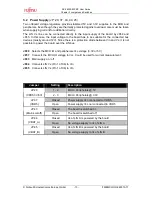
Page 13: ...s a protection diode between Vin and Vs it is not possible to power the board over the LIN bus JP29 Selects the MCU IO and peripherals Vcc voltage 3 3V or 5V JP37 Connects the MCU IO voltage to Vcc Could be used for current measurement JP43 Main supply on off JP44 Connects LIN Vs Pin 1 of X8 to Vin JP45 Connects LIN Vs Pin 1 of X6 to Vin Jumper Setting Description 1 2 MCU Peripherals 5V JP29 VDD5 ...

Page 14: ...c JP11 AVcc Open AVcc is disconnected from Vcc Closed AVRH is connected to AVcc JP13 AVRH Open AVRH defined by resistor network 1 Closed AVss is connected to GND JP15 AVss Open AVss is disconnected from GND 1 By default the resistors R11 and R23 are not mounted on the board Default JP11 JP13 and JP15 are closed By default the A D converter supply and reference voltage is same as the microcontrolle...

Page 15: ...efines usage of Pin 24 X0A P40 JP34 defines usage of Pin 25 X1A P41 Jumper Setting Description 1 2 Pin 24 is connected to the 32kHz Subclock X0A 2 4 Pin 24 is used as P4_0 and is connected to X4 B10 JP41 X0A P40 2 3 Pin 24 is connected to GND in case that subclock device is used but no 32kHz crystal is connected 1 2 Pin 25 is connected to the 32kHz Subclock X1A JP34 X1A P41 2 3 Pin 25 is used as P...

Page 16: ...ed RTS and CTS of X3 are connected JP31 RTS CTS Open RTS and CTS of X3 are not connected By default UART2 is connected to UART A 3 6 UART B JP 6 8 32 One RS232 transceiver U3 X5 can be connected to one of the microcontroller s UART interfaces JP6 JP8 connect UART 3 to the RS232 transceiver U3 X5 JP32 Some programs e g Terminals need a connection between CTS and RTS Jumper Setting Description Close...

Page 17: ...umper Setting Description Closed LIN transceiver is enabled JP17 LIN enable Open LIN transceiver is disabled Closed LIN Master mode JP18 LIN Master Open LIN Slave mode Closed SIN7 of the MCU is connected to LIN A JP21 LIN A RXD Open SIN7 of the MCU is not connected to LIN A Closed SOT7 of the MCU is connected to LIN A JP22 LIN A TXD Open SOT7 of the MCU is not connected to LIN A Closed Vs of LIN A...

Page 18: ...t connected to LIN B Closed SOT8 of the MCU is connected to LIN B JP39 LIN B TXD Open SOT8 of the MCU is not connected to LIN B Closed Vs of LIN B is powered by the board JP45 VBAT_B Open No voltage supply to Vs of LIN B 1 2 Connects WAKE signal to Bus power JP42 WAKE 2 3 Connects WAKE signal to VCC By default the LIN B interface is not connected to a UART 3 9 CAN A JP 19 25 26 One high speed CAN ...

Page 19: ...2 of MCU is connected to CAN B JP28 CAN A RX closed RX2 of MCU is connected to CAN B 1 2 CAN B VCC is set to 5V JP33 VCC CAN B 2 3 CAN B VCC is set to 3V3 3 11 I C Pull Up JP 46 47 Two 10k Ohm resistors can be connected to the SDA0 and SCL0 lines Jumper Setting Description JP46 SDA0 closed SDA0 is pulled up to VCC JP47 SCL0 closed SCL0 is pulled up to VCC 3 12 C Pin Capacitor For normal operation ...

Page 20: ...with this jumper Remove the jumper in order to disable the RS232 reset circuit Jumper Setting Description 1 2 DTR of UART A is selected JP3 DTR RTS A 2 3 RTS of UART A is selected 1 2 UART A is used to generate Reset JP4 UART A B 2 3 UART B is used to generate Reset 1 2 DTR of UART B is selected JP5 DTR RTS B 2 3 RTS of UART B is selected 1 2 Reset is applied immediately when SW6 is pressed JP7 Re...

Page 21: ...tion to the microcontroller Closed Pin 77 INT1 of the MCU is connected to SW2 JP14 SW2 Open No connection to the microcontroller Closed Pin 53 ATGR of the MCU is connected to SW3 JP16 SW3 Open No connection to the microcontroller Closed Pin 2 TIN1 of the MCU is connected to SW4 JP20 SW4 Open No connection to the microcontroller Closed Pin 4 NMIR of the MCU is connected to SW5 JP23 SW5 Open No conn...

Page 22: ...am the Flash ROM asynchronously the tool Fujitsu Flash MCU Programmer for FMC16FX can be used This tool is available free on the Fujitsu Micros DVD or Web Site http mcu emea fujitsu com select Software Utilities The following procedure must be followed to enable Flash Programming 1 Power off the board 2 Connect the Evaluation Board UART A or UART B to your serial PC communication port A straight 1...

Page 23: ...igure 4 1 Settings for Automatic Mode 7 The software now automatically writes a flash loader to the microcontroller Download does a blank check and erases the Flash memory if necessary After that the user application is programmed to the embedded Flash memory Program Verify 8 If the programming sequence has ended successfully you will receive the output It all ended normally completely 9 After pro...

Page 24: ... ROM synchronously special third party soft and hardware has to be used e g GALEP 4 from www conitec de This tool is not available for free A dedicated Flash programming socket X4 is provided on the evaluation board for direct connection to this programmer X17 Flash programming socket Figure 4 2 Flash Programming Socket nc 1 MD0 3 RSTX 5 SOT3 7 VCC 9 2 P00_1 4 nc 6 SIN3 8 SCK3 10 GND ...

Page 25: ...s except oscillator Pins of the microcontroller are directly connected to X1 and X2 as follows Connector MCU Pins X1 1 40 1 40 X2 41 80 41 80 The odd pin numbers are located on the one side and the even pin numbers are located on the other side of the connector 5 3 UART A UART B connector X3 X5 Two 9 pin D Sub female connectors are used for the serial interface UART A and UART B TXD is the transmi...

Page 26: ...terface Connector X10 5 6 USER LEDs optional LC Display Eight LEDs are supplied for user applications In order to disconnect the LEDs from the related microcontroller port the resistor network N1 can be removed Instead of the user LEDs an alphanumeric LC Display optional can be connected The following control signals are provided 14 13 12 11 10 9 8 7 6 5 4 3 2 1 LCD D7 D6 D5 D4 E R W RS V0 VCC GND...

Page 27: ...P05_5 JP23 SW5 65 21B P02_5 JP16 SW3 16 8B P05_6 66 21C P04_4 JP46 17 8C P05_7 67 22A P04_5 JP47 18 9A P07_0 JP12 SW1 68 22B P03_3 19 9B P04_2 JP26 CAN A 69 22C P03_1 20 10C P17_6 70 23A P03_2 JP28 CAN B 21 10A P04_3 JP25 CAN A 71 23B P03_3 JP27 CAN B 22 MCUVCC JP37 72 23C P03_4 23 VSS VSS 73 24A P03_5 24 X0A P04_0 JP41 74 24B P03_6 25 X1A P04_1 JP34 75 24C P03_7 26 MD2 S2 76 25A P13_6 27 MD1 S2 7...

Page 28: ...jitsu Microelectronics Europe GmbH 6 Silk Plot of the Board Power Jack UART A X3 MAX3232 MCU 96F326 4MHz VG96 male Pin 1 Pin 2 Pin 40 Pin 39 Pin 79 Pin 80 Pin 42 Pin 41 LIN A X8 CAN A X10 MAX3232 optional LCD SW1 SW2 SW3 SW4 SW5 Reset X1 X2 X12 FlashKit X17 LIN B X6 CAN B X11 UART B X5 ...

Page 29: ... 11 7 Revision and Error List The following bugs have been found with the board and need to be observed when working with this tool Date Revisions Errors Author Rev 18 04 2007 New document HWe DGo 1 0 18 04 2007 EMDC Design Spec Change RSTx at pin 57 former pin 55 Hand wire RST to pin 57 required for PCB V1 0 HWe 1 0 ...

Page 30: ...PT 80P M21 package MB2198 505 Probe cable MB2198 01 Emulator debugger main unit MB2198 500 Emulation Pod Adapter board NQPACK080SD ND Socket for package FPT 80P M21 Tokyo Eletech Corp http www tetc co jp HQPACK080SD Header for NQPACK080SD MB96320 Series MB96V300B MB96300 Series Evaluation chip MB96F326RS Flash MCU MB96320 Series single clock MB96F326RW Flash MCU MB96320 Series dual clock ...

Page 31: ...icrocontrollers 8 16 and 32bit Graphics Controllers Datasheets and Hardware Manuals Support Tools Hard and Software http mcu emea fujitsu com Power Management Products http www fujitsu com emea services microelectronics powerman Media Products SAW filters acoustic resonators and VCOs http www fujitsu com emea services microelectronics saw For more information about FUJITSU MICROELECTRONICS http ww...

Page 32: ...contains hazardous materials in excess of the limits established by the Chinese standard SJ T11363 2006 Requirements for Concentration Limits for Certain Hazardous Substances in Electronic Information Products The number in the symbol is the Environment friendly Use Period EFUP which indicates the period starting from the manufacturing date during which the toxic or hazardous substances or element...

Page 33: ...t be disposed of as unsorted municipal waste and must be collected separately and handled properly after decommissioning Please note The designation of 10 years EFUP is not to be equated with the durability use duration or any warranty claims of the product Table of hazardous substances name and concentration Hazardous substances name Component Name Pb Hg Cd Cr VI PBB PBDE SK 96320 80PMC x o o o o...

Page 34: ... wieder zurück Zur Entsorgung schicken Sie das Gerät bitte an die folgende Adresse Fujitsu Microelectronics Europe GmbH Warehouse Disposal Monzastraße 4a 63225 Langen Valid for European Union Countries According to the European WEEE Directive and its implementation into national laws we take this device back For disposal please send the device to the following address Fujitsu Microelectronics Euro...

Reviews: